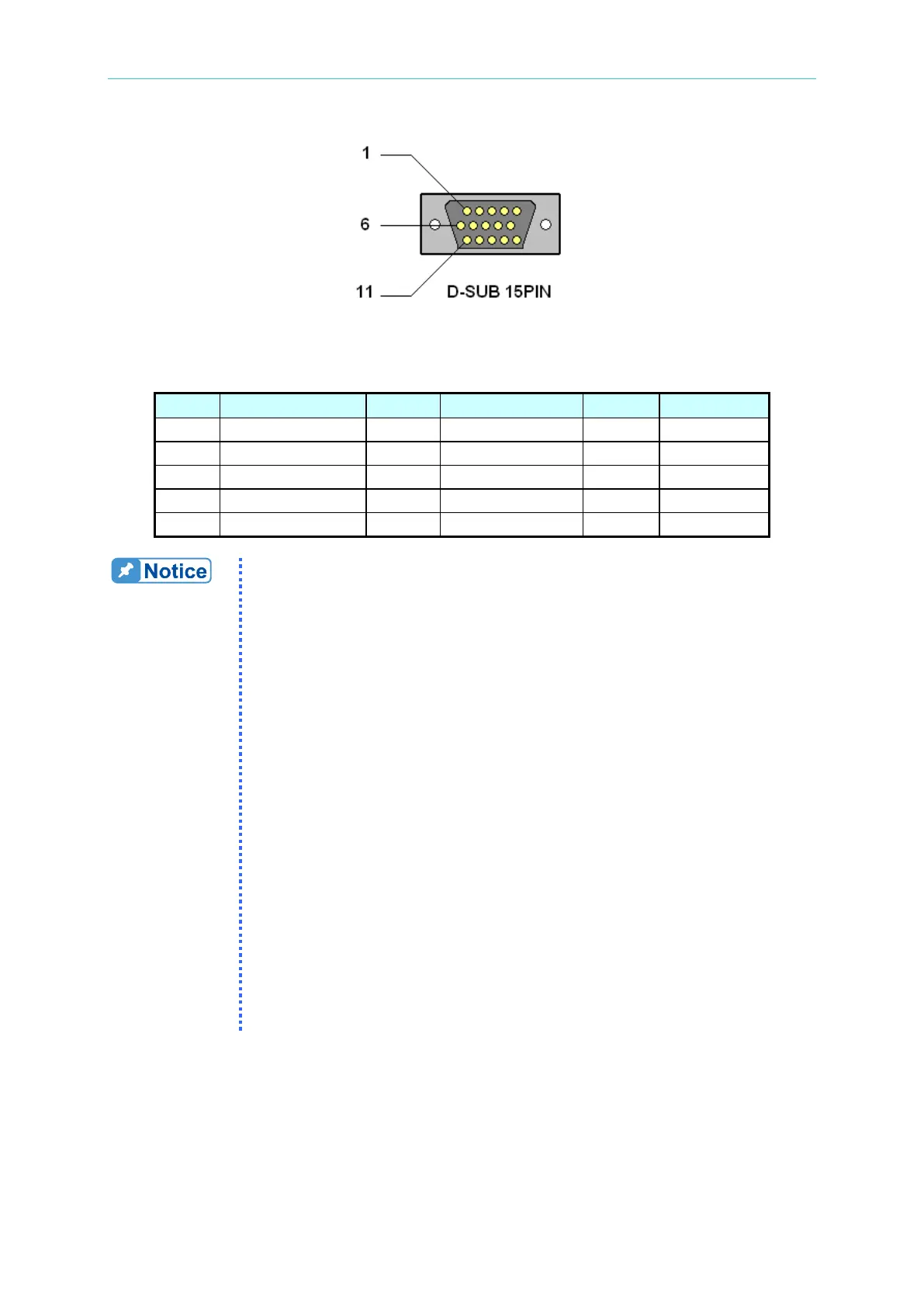
1. Pin [1:2]: EXT_WAVE[I:V] the external waveform input signal with
input range from 0 to 10V.
2. Pin [3:14:15]: the GND signal.
3. Pin [4]: SHORT ST the Short ON output signal, TTL Level and
Active High.
4. Pin [5]: the trigger source for TRIG_DIGI external trigger input signal
to be become digital. TTL Level, falling edge and pulse width ≥1μs.
5. Pin [6]: the Load ON output signal, TTL Level and Active High.
6. Pin [7]: TRIG_ SEQ the external input signal is automatically
triggered in the following sequence: TTL Level, falling edge, and
pulse width ≥1μs.
7. Pin [8:9]: DO[1:2] the binary digital output signal, high level: 4.7kΩ
resistance increases to 5V, low level <0.6V, loading current = 10mA.
8. Pin [10]: DO3
9. Pin [11:12]: DI[1:2] provides External Load ON/OFF function so that
the user can use the input signal to control Load ON/OFF externally.
When DI1 and DI2 are both set to External Load ON/OFF, both
signals need to be HIGH to Load OFF and on the contrary both
signals need to be LOW to Load ON.
When DI1 (or DI2) is set to Remote Inhibit and Low, all channels in
the Electronic Load are Load OFF and a message of REMOTE
INHIBIT will appear. If this protection is not cleared, even the DI1 (or
DI2) is High, Load on cannot be executed. DI1 and DI2 are for
communication control and the action time should be less than 5ms.
 Loading...