FSG/MTM/001 060511
39
3.6 Check and Adjustment of Camera Board, CBF (Tx and XL models)
All test points referred to are shown in Fig. 3-6, page 41.
All voltages are measured relative to test point GND.
CBF Block Diagram is shown in Fig. 3-7, page 42.
3.6.1 DC Voltages
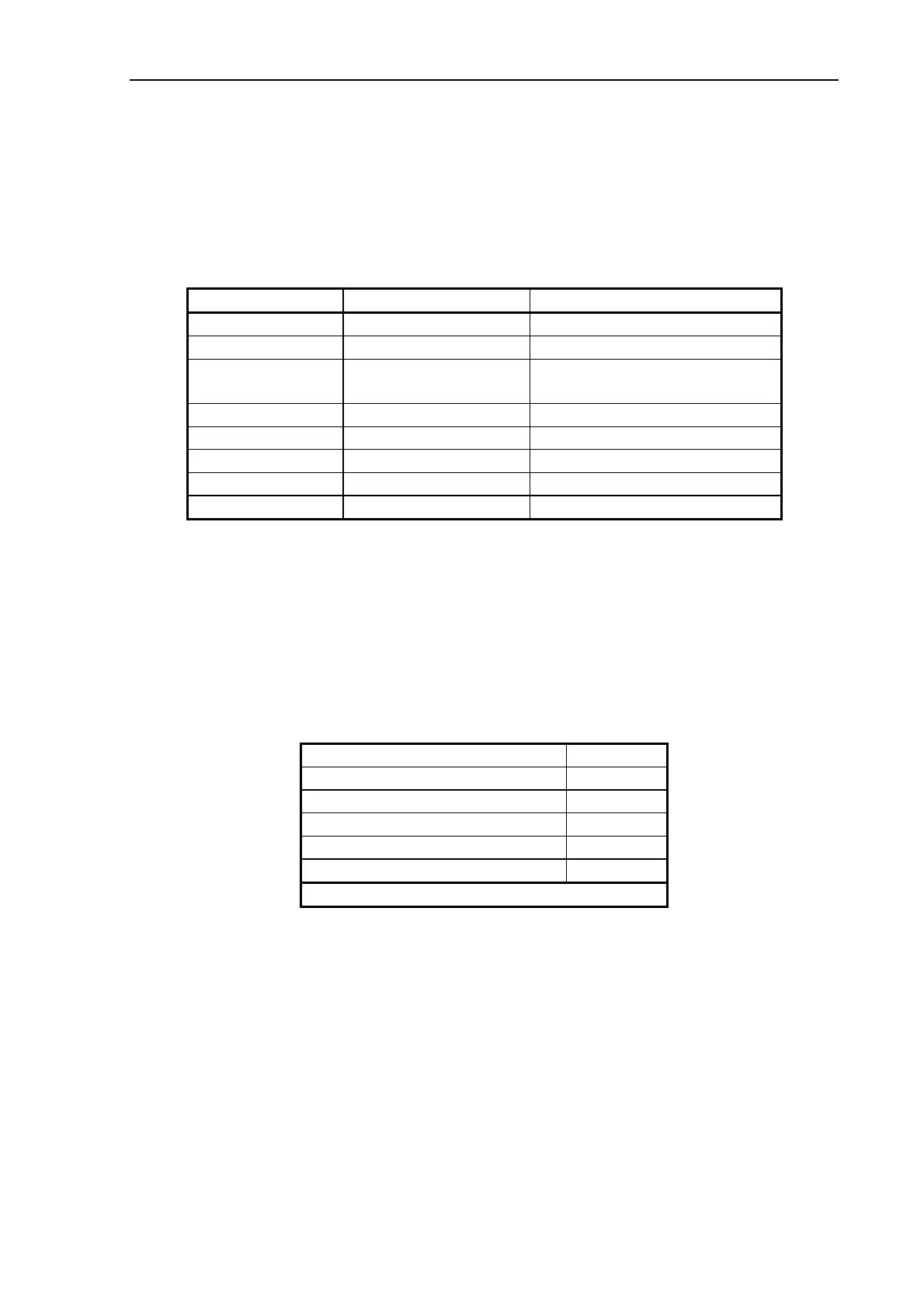
Ref. on Fig. 3-6 DC Voltage Remarks
C918, bottom +5.3 V +0/-0.2 V From SUC / SMPS
C901, bottom +3.3 V ± 0.1 V From SUC / SMPS
IC1101, pin 19 +12.0 V +1/-0 V From SUC / SMPS, used for
CCD and Camera Motor
C921, bottom +5 V ± 0.2 V From On-Board Regulators
C917, left +5 V ± 0.2 V From On-Board Regulators
C913, bottom +5 V ± 0.2 V From On-Board Regulators
C905, top +2.5 V ± 0.1 V From On-Board Regulators
Q102, bottom +11.6 V ± 0.6 V From On-Board Regulators
3.6.2 Adjustments
The gain and offset of the CBF-Board are adjusted automatically by running Scanner
Maintenance.
3.6.3 Functional Test
SCANtest 6: Test 7, Complete Hardware Test
3.6.4 Markings
CHROMA Tx 40
CBFAdd
CRYSTAL Tx 40
CBFAdd
MAGNUM XL 54
CBFAdd
COUGAR Tx 36
CBFAdd
CHAMELEON Tx 36
CBFAdd
PREMIER Tx 36
CBFAdd
where dd = board revision number.
3.6.5 Jumper Settings
No jumpers.
3.6.6 Hints
+3.3 V, +5.3 V, and +12 V is supplied from the SMPS via the SUC-Board.
On-Board Regulators are supplied from the SMPS via the SUC-Board.
CCD
The lines of pixels on the CCD are arranged as follows:
Upper line on the CCD: Red
2nd line on the CCD: Green
 Loading...