Register file: 0x26 – GPIO control and status, sub-register 0x04 is reserved.
7.2.39.3 Sub-Register 0x26:08 – GPIO_DIR
GPIO Direction control register
Register file: 0x26 – GPIO control and status, sub-register 0x08 is the GPIO Direction Control Register,
GPIO_DIR. The GPIO_DIR register applies to the GPIO pins when they are selected to operate as GPIOs via
the GPIO_MODE register. It contains a bit for each GPIO to individually configure that GPIO as an input or
an output. The register is designed to allow software to change the direction of a single pin without
knowing the settings needed for other pins. This is achieved by having for each direction selection bit (GDP)
an associated mask bit (GDM) used to qualify the write to the GDP direction bit. This allows an individual
direction to be changed in the register without affecting other direction bits. Note that when reading from
this register only the direction GDP bits are returned and these are packed into the lower 9 bits. A GDP
direction bit value of 1 means the pin is an input. A GDP bit value of 0 means the pin is an output. The GDP
bits and their corresponding GDM mask bits are arranged with four GPIO per octet to allow a single octet
write to change direction of an individual GPIO.
The GPIO_DIR register contains the following sub-fields:
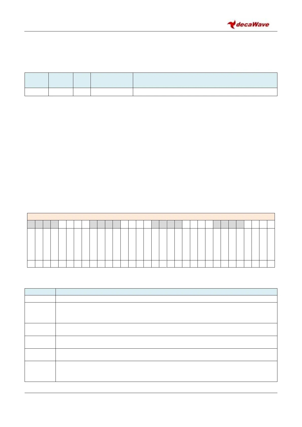
REG:26:08 – GPIO_DIR – GPIO Direction control register
The fields of the GPIO_DIR register identified above are individually described below:
Description of fields within Sub-Register 0x26:08 – GPIO_DIR
Bits marked ‘-’ in are reserved and should be written as zero.
Direction Selection for GPIO0. Reading this bit shows the direction setting for GPIO0.Values
1 = input, 0 = output. When writing (either 1 or 0) this GDP0 value is only changed if the GDM0
mask bit has a value of 1 for the write operation.
Direction Selection for GPIO1. (See GDP0).
Direction Selection for GPIO2. (See GDP0).
Direction Selection for GPIO3. (See GDP0).
Mask for setting the direction of GPIO0. When writing to GDP0 so select the I/O direction of
GPIO0, the value of GDP0 is only changed if this GDM0 mask bit has a value of 1 for the write
operation. GDM0 will always read as 0.