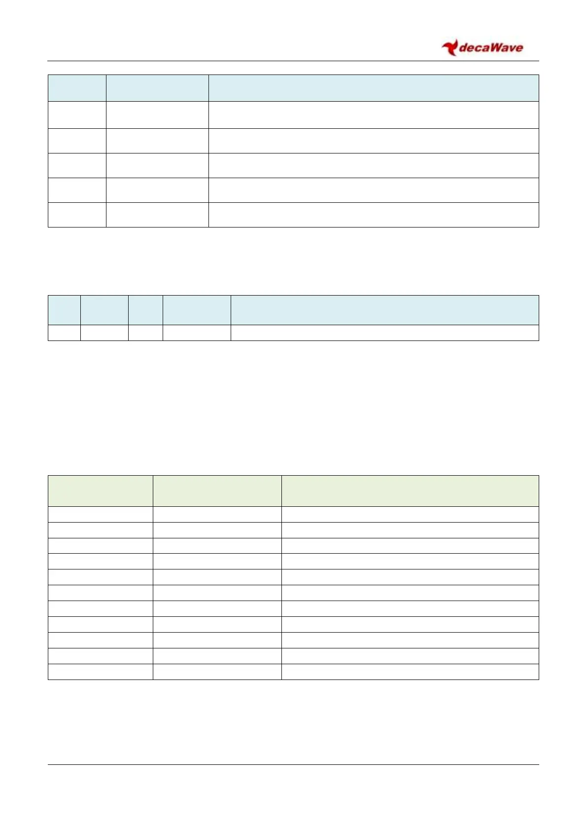
Description of fields within Register file: 0x25 – Accumulator CIR
memory
Low 8 bits of real part of accumulator sample 1015
(1016
th
and last sample of CIR for the nominal 64 MHz mean PRF)
High 8 bits of real part of accumulator sample 1015
(1016
th
and last sample of CIR for the nominal 64 MHz mean PRF)
Low 8 bits of imaginary part of accumulator sample 1015
(1016
th
and last sample of CIR for the nominal 64 MHz mean PRF)
High 8 bits of imaginary part of accumulator sample 1015
(1016
th
and last sample of CIR for the nominal 64 MHz mean PRF)
NB: Because of an internal memory access delay when reading the accumulator the first octet output is a
dummy octet that should be discarded. This is true no matter what sub-index the read begins at.
7.2.39 Register file: 0x26 – GPIO control and status
Peripheral register bus 1 access - GPIO control
Register map register file 0x26 is concerned with the use of the GPIO. It contains a number of sub-registers.
An overview of these is given by Table 28. Each of these sub-registers is separately described in the sub-
sections below.
Note: the GPIO clocks need to be turned on, before enabling or disabling the GPIO mode or value. The
GPIO clocks are enabled by setting GPCE and GPRN in PMSC_CTRL0
Table 28: Register file: 0x26 – GPIO control and status overview
GPIO Mode Control Register
GPIO Direction Control Register
GPIO Data Output register
GPIO Interrupt Sense Selection
GPIO Interrupt Mode (Level / Edge)
GPIO Interrupt “Both Edge” Select
GPIO Interrupt Latch Clear
GPIO Interrupt De-bounce Enable


 To Next Page