Description of fields within Sub-Register 0x26:20 – GPIO_ICLR
GPIO IRQ latch clear for GPIO7 input. Write 1 to clear the interrupt latch.
GPIO IRQ latch clear for GPIO8 input. Write 1 to clear the interrupt latch.
Bits marked ‘-’ are reserved and should be written as zero.
7.2.39.10 Sub-Register 0x26:24 – GPIO_IDBE
GPIO Interrupt De-bounce Enable
Register file: 0x26 – GPIO control and status, sub-register 0x24 is the GPIO interrupt de-bounce enable
register. The GPIO_IDBE controls a filtering function that operates on the GPIO inputs prior to their
presentation into the GPIO interrupt logic. This de-bounce filter circuit removes short transients by using the
kilohertz clock (as enabled by the KHZCLKEN bit in Sub-Register 0x36:00 – PMSC_CTRL0) to sample the input
signal. See KHZCLKDIV in Sub-Register 0x36:04 – PMSC_CTRL1 for a description of the kilohertz clock. The
de-bounce filter is active when a state change of the GPIO input needs to persist for two cycles of this clock
before it will be seen by the interrupt handling logic. The GPIO_IDBE register contains a bit for each GPIO
pin as follows:
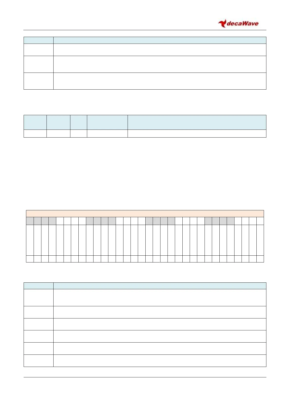
REG:26:24 – GPIO_IDBE – GPIO Interrupt De-Bounce Enable
The bits of the GPIO_IDBE register identified above are individually described below:
Description of fields within Sub-Register 0x26:24 – GPIO_IDBE
GPIO IRQ de-bounce enable for GPIO0. Value 1 = de-bounce enabled. Value 0 = de-bounce
disabled.
GPIO1 IRQ de-bounce configuration. Value 1 = de-bounce enabled, 0 = de-bounce disabled.
GPIO2 IRQ de-bounce configuration. Value 1 = de-bounce enabled, 0 = de-bounce disabled.
GPIO3 IRQ de-bounce configuration. Value 1 = de-bounce enabled, 0 = de-bounce disabled.
GPIO4 IRQ de-bounce configuration. Value 1 = de-bounce enabled, 0 = de-bounce disabled.
GPIO5 IRQ de-bounce configuration. Value 1 = de-bounce enabled, 0 = de-bounce disabled.