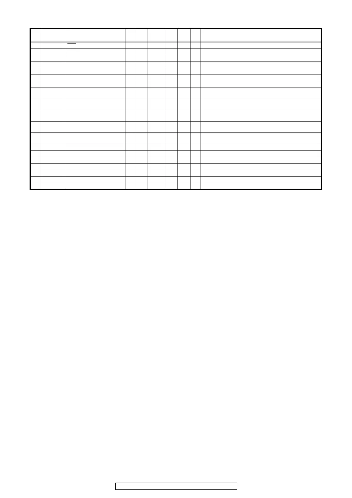
71
AVR-3808CI / AVR-3808 / AVC-3808
82 P04/D4 INT2 I-E↓&L-EdZ
DIRcontrolpin(LC89057W-VF4-E)
83 P03/D3 INT1 I-E↓&L-EdZ
DIRcontrolpin(LC89057W-VF4-E)
84 P02/D2 DIRRST3 O C - - - Z
DIRcontrolpin(LC89057W-VF4-E)
85 P01/D1 DIRRST2 O C - - - Z
DIRcontrolpin(LC89057W-VF4-E)
86 P00/D0 DIRRST1 O C - - - Z
DIRcontrolpin(LC89057W-VF4-E)
87 P107/AN7 DSP2RST O C - - Ed Z
DSP2(ADSP-21367)resetoutputpin(reset:L)
88 P106/AN6 DSP1RST O C - - Ed Z
DSP1(ADSP-21366)resetoutputpin(reset:L)
89 P105/AN5 DSPROMRST/SUBnCE O C - - Ed Z
DSPmemoryreset(reset:L)/FPGArewritecontrol(MAINFPGA&GUI
FPGAcombineduse)
90 P104/AN4 DSP1FLAG0/SUBDATAO I - Lv - Ed Z
DSP1controlpin(ADSP-21366)/FPGArewritecontrol(MAINFPGA&GUI
FPGAcombineduse)
91 P103/AN3 DSP2FLAG0/SUBCONFDONE I - Lv - Ed Z
DSP1controlpin(ADSP-21367)/FPGArewritecontrol(MAINFPGA&GUI
FPGAcombineduse)
92 P102/AN2 DSP2ICS/SUBnCS O C - - Eu Z
DSP1controlpin(ADSP-21367)/FPGArewritecontrol(MAINFPGA&GUI
FPGAcombineduse)
93 P101/AN1 DSP1ICS/SUBASDI O C - - Eu Z
DSP1controlpin(ADSP-21366)/FPGArewritecontrol(MAINFPGA&GUI
FPGAcombineduse)
94 AVSS AVSS - - - - - -
ADGND
95 P100/AN0 /SUBDCLK O C - - - Z
/FPGArewritecontrol
96 VREF VREF - - - - - -
ADref.+3.3V
97 AVCC AVCC - - - - - -
AD+3.3V
98 P97/SIN4 DSPMISO I - Lv - Eu Z
DSPcontrolpin(ADSP-21366)/(ADSP-21367)
99 P96/SOUT4 DSPMOSI O C - - Eu Z
DSPcontrolpin(ADSP-21366)/(ADSP-21367)
100 P95/CLK4 DSPICLK O C - - Eu Z
DSPcontrolpin(ADSP-21366)/(ADSP-21367)
Pin PinName Symbol I/O Type Det
Op
(Int.)
Op
(Ext.)
Res
Function
Note: Pin No. : Terminal number of microcomputer.
Port Name : The name entered in the data sheet of microcomputer.
Symbol : Symbolized interface function.
I/O : Input or out of part.
“I” = Input port
“O” = Output port
Type : Composition of port in case of output port.
“C” = CMOS output
“N” = NMOS open drain output
“P” = PMOS open drain output
Op : Pull up/Pull down selection information.
“Iu” = Inner microcomputer pull up
“Id” = Inner microcomputer pull down
“Eu” = External microcomputer pull up
“Ed” = External microcomputer pull down
Det : Indicates judging state of input port. Level detection is “LV”; Edge detection is “Ed”; Detection by both shifting is “E&L”;
Serial data detection is “S” (Serial data output is also “S”).
Res : State at reset.
“H” = Outputs High Level at reset
“L” = Outputs Low Level at reset
“Z” = Becomes High impedance mode at reset
STBY : State of port when STANDBY mode.
“O/L” = Output port and “L”
“I” = Input port
Stop : State of port when Stop mode.
“O/L” = Output port and “L”
“I” = Input port
 Loading...