04/10 MN04020001Z-EN
Parameter menu (PAR)
75
Analog input (P2)
In parameter group P2, you can adapt the analog inputs:
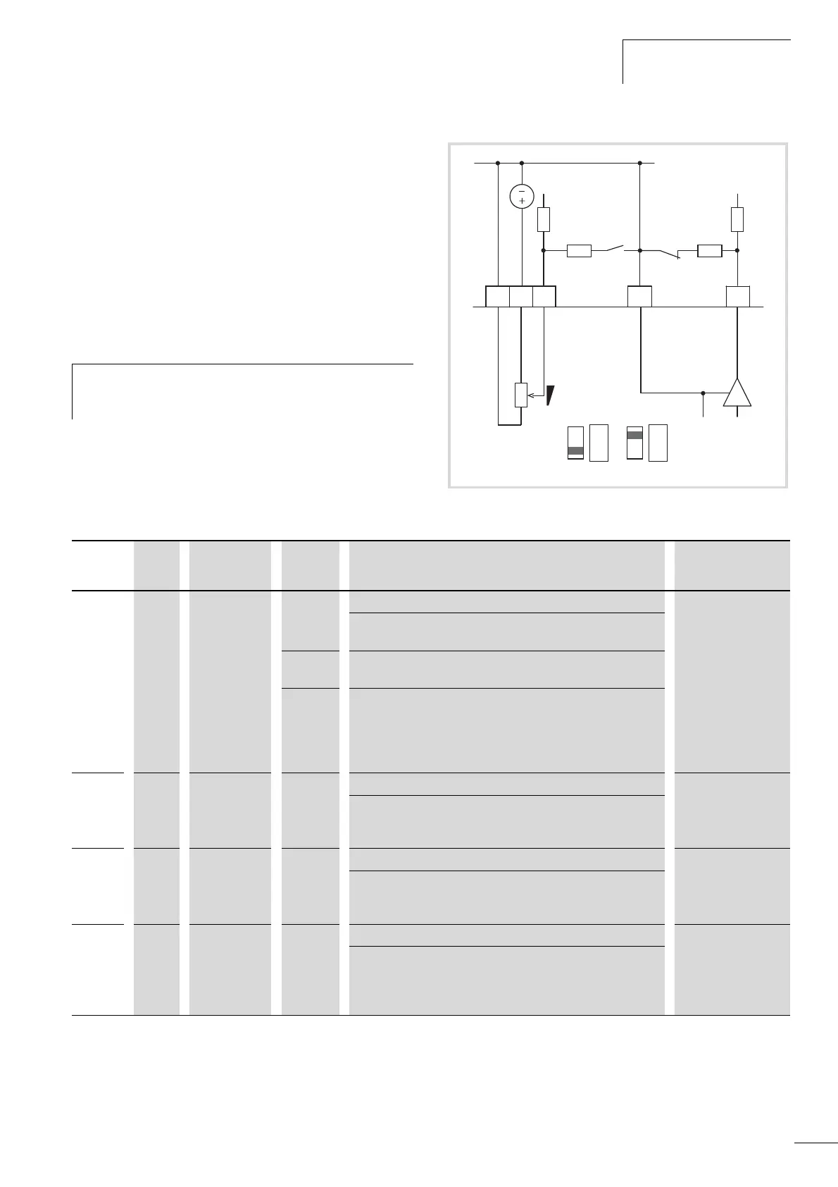
The signal range depends on the switch position of the
microswitches (see figure 68):
• S2 = V: AI1 (control signal terminal 2), voltage signal
0/2 - +10 V.
• S3 = mA: AI2 (control signal terminal 4), current signal
0/4 - 20 mA.
Reference potential for the analog inputs (AI1, AI2) is GND
(control signal terminals 3 and 5).
h
The allocation of the analog inputs (AI1, AI2) can be set
under parameter P6.2 and P6.18 (setpoint input) as well
as P9.5 and P9.6 (PI controller, actual value).
Figure 68: Analog inputs AI1 and AI2
12354
0 (4)...20 mA
AI1
GND
< 10 mA
+10 V Out
S3S2
GND
0...+10 V
200 kO 200 kO
200 O 200 O
AI2
PI-Ist
f-Soll
S2 = AI1 V
(0...+10 V)
AI1
V mA
S3 = AI2 mA
(4...20 mA)
AI1
V mA
PNU ID Access right
RUN
Value Description Factory setting
(P1.3)
P2.1 379 / AI1 Signal range (Analog input). 0
Depending on the switch position of microswitch S2
(FS = frequency setpoint).
0 S2 = V: 0 - +10 V, voltage signal (FS, a P6.2).
S2 = mA: 0 - 20 mA, current signal.
1 With live-zero,
S2 = V: 2 - +10 V, voltage signal,
S2 = mA: 4 - 20 mA, current signal.
a At P8.1 it is possible to set the response of the MMX to a
setpoint error (life zero).
P2.2 380 / AI1 Custom Min 0.00
Scaling (-100.00 % - 100.00 %) of the analog input signal (V/mA)
in the zero range (minimum response value).
a section “Scaled value range (AI1, AI2)”, page 76.
P2.3 381 / AI1 Custom Max 100.00
Scaling (-100.00 % - 100.00 %) of the analog input signal (V/mA)
in the limit value range (highest limit value).
a section “Scaled value range (AI1, AI2)”, page 76.
P2.4 378 / AI1 Filter time 0.1
0.0 no filter function.
0.1 - 10.0 s = Filter time constant for the analog input signal
(V/mA).
a section “Filter time constant”, page 77.
 Loading...