A201A
VOLTAGE CONTROL OSCILLATOR
(2020142)
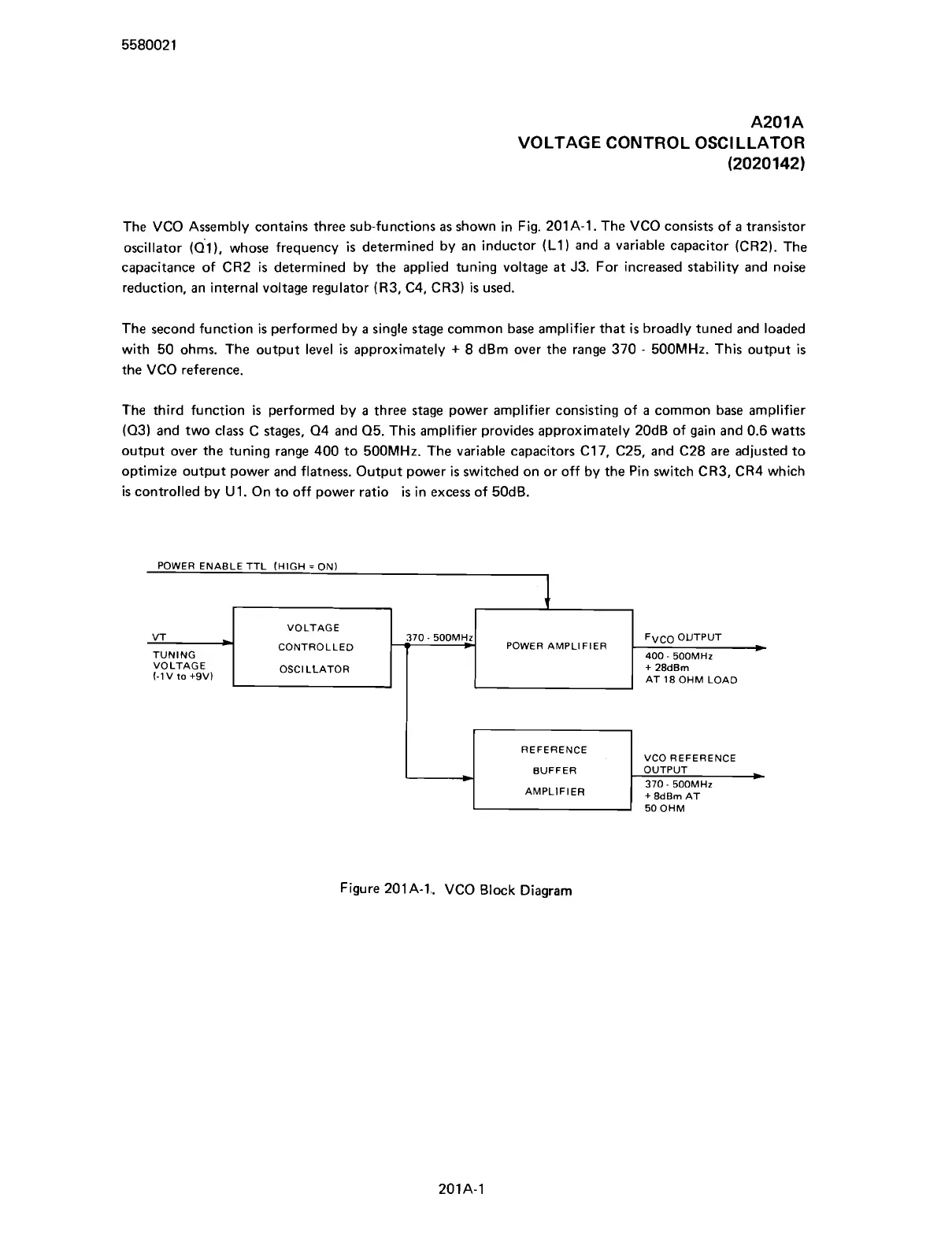
The VCO Assembly contains three sub-functions as shown in Fig. 201A-1. The VCO consists of a transistor
oscillator
(dl), whose frequency
is
determined by an inductor (L1) and a variable capacitor (CR2). The
capacitance of CR2
is
determined by the applied tuning voltage at J3. For increased stability and noise
reduction, an internal voltage regulator
(R3, C4, CR3)
is
used.
The second function
is
performed by a single stage common base amplifier that
is
broadly tuned and loaded
with 50 ohms. The output level
is
approximately
+
8 dBm over the range 370
-
500MHz. This output
is
the VCO reference.
The third function
is
performed by a three stage power amplifier consisting of a common base amplifier
(03) and two class C stages, 04 and 05. This amplifier provides approximately 20dB of gain and 0.6 watts
output over the tuning range 400 to
500MHz. The variable capacitors C17, C25, and C28 are adjusted to
optimize output power and flatness. Output power
is
switched on or off by the Pin switch CR3, CR4 which
is
controlled by U1. On to off power ratio
is
in excess of 50dB.
POWER ENABLE TTL (HIGH
=
ON)
I
Figure 201 A-1,. VCO Block Diagram
VT
-.
TUNING
VOLTAGE
(-1
V
to
+9V)
REFERENCE
BUFFER
AMPLIFIER
VCO REFERENCE
OUTPUT
L
370
-
500MHz
+
8dBm AT
50 OHM
VOLTAGE
CONTROLLED
OSCl LLATOR
370
-
500MHz
T
-
POWER AMPLIFIER
FVCO OUTPUT
.
W
400
-
500MHz
+
28dBm
AT 18 OHM LOAD
Scans by ArtekMedia © 2007