EPSON Perfection V10/V100 Photo/V200 Photo/V350 Photo Revision B
OPERATING PRINCIPLES Control Circuit 25
2.2 Control Circuit
The Control Circuit of this scanner consists of the following circuits.
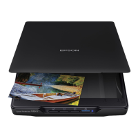
MAIN UNIT
(PERFECTION V10/PERFECTION V100 PHOTO/PERFECTION V350 PHOTO)
Main Board B184MAIN (Perfection V10)
B184MAINB (Perfection V100 Photo/Perfection V350 Photo)
CCD Board B184ISN (Perfection V10/Perfection V100 Photo)
B185ISN (Perfection V350 Photo)
PNL Board B184PNL
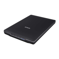
MAIN UNIT
(PERFECTION V200 PHOTO)
Main Board B188MAIN
CCD Board B188ISN
PNL Board B188PNL
AFL (PERFECTION V350 PHOTO)
AFL Main Board B185DRV
2.2.1 Image Processing Operation
The sequence of scanned image processing is explained in order below.
1. CCD Board (CCD Image Sensor)
Optoelectronic transformation processing (reflected light (optical energy)
from a document surface is transformed into electric charge (electric energy))
Amplification processing
2. Main Board (scanned image data processing)
A/D conversion processing (scanned image data generated as an analog
electric signal is converted to a digital signal)
Shading correction processing (scanned image data is corrected on the basis
of the white and black reference values)
Various image correction processing (gamma correction, color correction,
halftone correction, etc. are executed under the set conditions from the host
side)
3. The above processing is performed and the scanned image data are output to the host
side at the end.
 Loading...