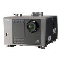
“Confidential, Do Not Duplicate without written authorization from NEC.”
8-32
CIRCUIT DESCRIPTION
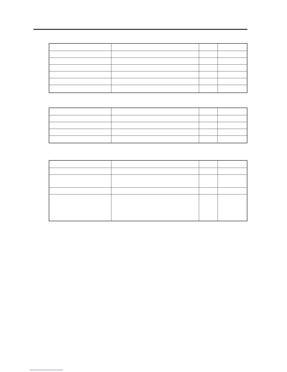
Signal Name Description I/O Type
DCLK_C [P, N] DMD Port C Differential Clock O 2.5V LVDS
DCLK_D [P, N] DMD Port D Differential Clock O 2.5V LVDS
SCTRL_C [P, N] DMD Port C Differential Serial Control O 2.5V LVDS
SCTRL_D [P, N] DMD port D Differential Serial Control O 2.5V LVDS
DATA_C [P, N] (15:0) DMD Port C Differential Serial Data O 2.5V LVDS
DATA_D [P, N] (15:0) DMD Port D Differential Serial Data O 2.5V LVDS
1-3. DMD LVDS Interface
Signal Name Description I/O Type
SCP_CK SCP Bus Clock O 3.3V LVTTL
SCP_DO SCP Bus Output Data O 3.3V LVTTL
SCP_DI SCP Bus Input Data I 3.3V LVTTL
SCP_DMD_ENZ SCP Bus DMD Enable (Active LOW) O 3.3V LVTTL
1-4. DMD Serial Communications Port Interface
Signal Name Description I/O Type
DMD_PWRDNZ DMD Reset (Active LOW) O 3.3V LVTTL
SIGNAL_ASIC_EN Signal ASIC configuration Enable O 3.3V LVTTL
(Active HIGH)
DMD_MODE_[A, B] DMD Bandwidth Mode select O 3.3V LVTTL
MBRST (29:0) Non-logic compatible Mirror Bias Reset O —
signals Connected directly to the array
of pixel mirrors
Used to hold or release the mirrors
1-5. DMD Reset and Mode Control