9-26
“Confidential, Do Not Duplicate without written authorization from NEC.”
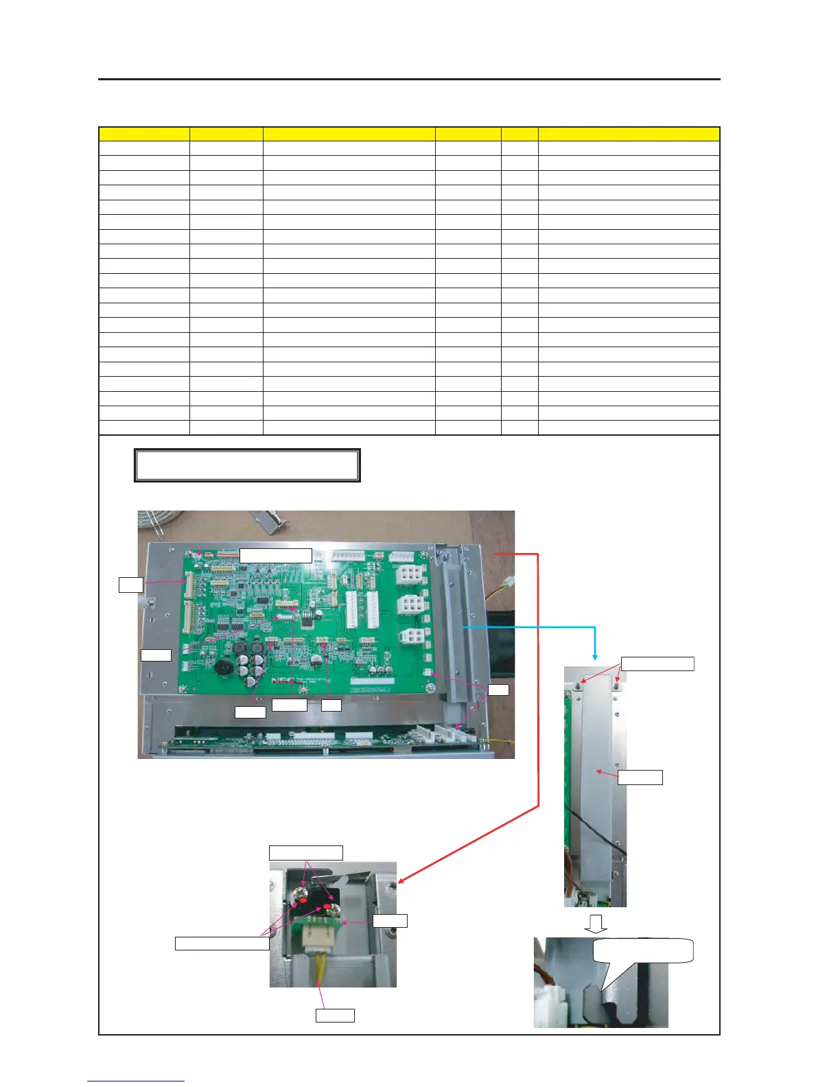
ASSEMBLY DIAGRAM
Diagram symbol Circuit symbol Part name Part code Q’ty Remarks
PWB1 ETC3 PWB PWB ASSY 81N94Z01 1
SRW143 CBIMS*2*8*3GF 24V01031 2 Torque check
T1 CN3P(T1)225W,1061-26 7NW3W089 1
TA CN2P(TA)100W,1061-26 7NW2W058 1
PU CN3P(PU)925W,3265-24 7NW3W087 1
PSC CN5P(PSC)875W,1061-26 7NW5W064 1
SIO CN5P(SIO)200W,1061-24 7NW5W068 1
J100 CN8P(J100)500W,1061-24 7NW8W032 1
F1 CN12-WP(F1)250X,1061-24 7NWBV005 1
PRT1 SHIELD CASE D 24H61032 1
SRW044 SCREW,PL-CPIMS*3*8*3GF 24V00111 2
GULE,SCREW LOCK 92201082
TI BOX4
J100
SIO
1 Insert each CONNECTOR into PJDIV PWB ASSY. (Picture below)
2 Insert CN(TA) into "PO6013" between PJDIV - MOTHER PWB ASSY.
3 Set CN(T1) into TI Shiled Case after inserting TAMPER PWB ASSY.
4 Set Shiled Case D over CN(T1) after setting on TAMPER PWB ASSY.
Make sure not to pinch this connector with the Shield Case D.
SRW143 X2P
F1
PU
PSC
[CAUTION] countermeasure against static electricity
Use WRISTSTRAP when handling the BOARD.
TA
CN(T1)
SRW143 X2P
PRT1
SRW044 X2P
GLUE,SCREW LOCK
PWB
The lower side shall
be hung on the hook.