LPC5411x All information provided in this document is subject to legal disclaimers. © NXP Semiconductors N.V. 2018. All rights reserved.
Product data sheet Rev. 2.1 — 9 May 2018 15 of 105
NXP Semiconductors
LPC5411x
32-bit ARM Cortex-M4/M0+ microcontroller
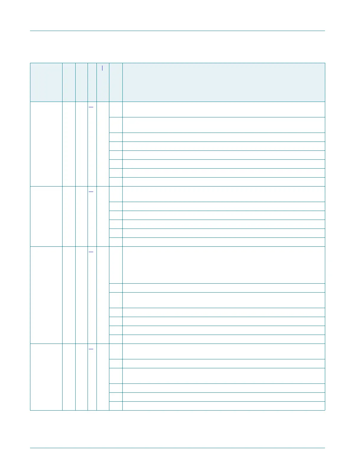
PIO0_29/
ADC0_0
D3 11
[4]
PU I/O;
AI
PIO0_29/ADC0_0 — General-purpose digital input/output pin. ADC input channel 0
if the DIGIMODE bit is set to 0 in the IOCON register for this pin.
I/O FC1_RXD_SDA_MOSI — Flexcomm Interface 1: USART RXD, I2C SDA, SPI
MOSI.
O SCT0_OUT2 — SCT0 output 2. PWM output 2.
O CTimer0_MAT3 — 32-bit CTimer0 match output 3.
R — Reserved.
I CTimer0_CAP1 — 32-bit CTimer0 capture input 1.
R — Reserved.
O CTimer0_MAT1 — 32-bit CTimer0 match output 1.
PIO0_30/
ADC0_1
C1 12
[4]
PU I/O;
AI
PIO0_30/ADC0_1 — General-purpose digital input/output pin. ADC input channel 1
if the DIGIMODE bit is set to 0 in the IOCON register for this pin.
I/O FC1_TXD_SCL_MISO — Flexcomm Interface 1: USART TXD, I2C SCL, SPI MISO.
O SCT0_OUT3 — SCT0 output 3. PWM output 3.
O CTimer0_MAT2 — 32-bit CTimer0 match output 2.
R — Reserved.
I CTimer0_CAP2 — 32-bit CTimer0 capture input 2.
PIO0_31/
ADC0_2
C2 13
[4]
PU I/O;
AI
PIO0_31/ADC0_2 — General-purpose digital input/output pin. ADC input channel 2
if the DIGIMODE bit is set to 0 in the IOCON register for this pin.
Remark: This pin is also used to invoke ISP mode after device reset. Secondary
selection of boot source for ISP mode also uses PIO0_4 and PIO1_6. See the Boot
Process chapter in UM10914 for more details.
O PDM0_CLK — Clock for PDM interface 0, for digital microphone.
I/O FC2_CTS_SDA_SSEL0 — Flexcomm Interface 2: USART CTS, I2C SDA, SPI
SSEL0.
I CTimer2_CAP2 — 32-bit CTimer2 capture input 2.
R — Reserved.
I CTimer0_CAP3 — 32-bit CTimer0 capture input 3.
O CTimer0_MAT3 — 32-bit CTimer0 match output 3.
PIO1_0/
ADC0_3
C3 14
[4]
PU I/O;
AI
PIO1_0/ADC0_3 — General-purpose digital input/output pin. ADC input channel 3 if
the DIGIMODE bit is set to 0 in the IOCON register for this pin.
I PDM0_DATA — Data for PDM interface 0, digital microphone input.
I/O FC2_RTS_SCL_SSEL1 — Flexcomm Interface 2: USART RTS, I2C SCL, SPI
SSEL1.
O CTimer3_MAT1 — 32-bit CTimer3 match output 1.
R — Reserved.
I CTimer0_CAP0 — 32-bit CTimer0 capture input 0.
Table 4. Pin description
…continued
Symbol
49-pin
64-pin
Reset state
[1]
Type
Description

 Loading...


