LPC5411x All information provided in this document is subject to legal disclaimers. © NXP Semiconductors N.V. 2018. All rights reserved.
Product data sheet Rev. 2.1 — 9 May 2018 16 of 105
NXP Semiconductors
LPC5411x
32-bit ARM Cortex-M4/M0+ microcontroller
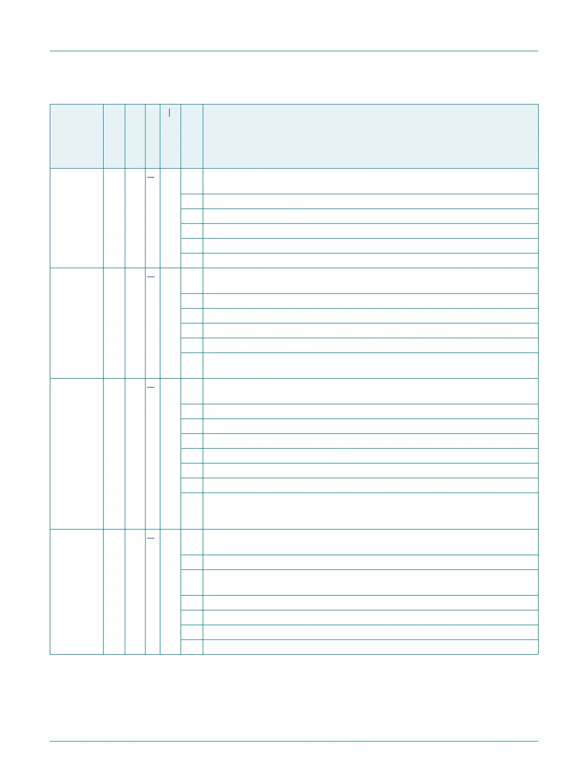
PIO1_1/
ADC0_4
B1 15
[4]
PU I/O;
AI
PIO1_1/ADC0_4 — General-purpose digital input/output pin. ADC input channel 4 if
the DIGIMODE bit is set to 0 in the IOCON register for this pin.
R — Reserved.
I/O SWO — Serial wire trace output.
O SCT0_OUT4 — SCT0 output 4. PWM output 4.
I/O FC5_SSEL2 — Flexcomm Interface 5: SPI SSEL2.
I/O FC4_TXD_SCL_MISO — Flexcomm Interface 4: USART TXD, I2C SCL, SPI MISO.
PIO1_2/
ADC0_5
A1 16
[4]
PU I/O;
AI
PIO1_2/ADC0_5 — General-purpose digital input/output pin. ADC input channel 5 if
the DIGIMODE bit is set to 0 in the IOCON register for this pin.
I/O MCLK — MCLK input or output for I2S and/or digital microphone.
I/O FC7_SSEL3 — Flexcomm Interface 7: SPI SSEL3.
O SCT0_OUT5 — SCT0 output 5. PWM output 5.
I/O FC5_SSEL3 — Flexcomm Interface 5: SPI SSEL3.
I/O FC4_RXD_SDA_MOSI — Flexcomm Interface 4: USART RXD, I2C SDA, SPI
MOSI.
PIO1_3/
ADC0_6
B2 17
[4]
PU I/O;
AI
PIO1_3/ADC0_6 — General-purpose digital input/output pin. ADC input channel 6 if
the DIGIMODE bit is set to 0 in the IOCON register for this pin.
R — Reserved.
I/O FC7_SSEL2 — Flexcomm Interface 7: SPI SSEL2.
O SCT0_OUT6 — SCT0 output 6. PWM output 6.
R — Reserved.
I/O FC3_SCK — Flexcomm Interface 3: USART or SPI clock.
I CTimer0_CAP1 — 32-bit CTimer0 capture input 1.
O USB_UP_LED — USB port 2 GoodLink LED indicator. It is LOW when the device is
configured (non-control endpoints enabled). It is HIGH when the device is not
configured or during global suspend.
PIO1_4/
ADC0_7
A2 18
[4]
PU I/O;
AI
PIO1_4/ADC0_7 — General-purpose digital input/output pin. ADC input channel 7 if
the DIGIMODE bit is set to 0 in the IOCON register for this pin.
O PDM1_CLK — Clock for PDM interface 1, for digital microphone.
I/O FC7_RTS_SCL_SSEL1 — Flexcomm Interface 7: USART RTS, I2C SCL, SPI
SSEL1.
O SCT0_OUT7 — SCT0 output 7. PWM output 7.
R — Reserved.
I/O FC3_TXD_SCL_MISO — Flexcomm Interface 3: USART TXD, I2C SCL, SPI MISO.
O CTimer0_MAT1 — 32-bit CTimer0 match output 1.
Table 4. Pin description
…continued
Symbol
49-pin
64-pin
Reset state
[1]
Type
Description

 Loading...


