LPC5411x All information provided in this document is subject to legal disclaimers. © NXP Semiconductors N.V. 2018. All rights reserved.
Product data sheet Rev. 2.1 — 9 May 2018 70 of 105
NXP Semiconductors
LPC5411x
32-bit ARM Cortex-M4/M0+ microcontroller
[1] Based on characterization; not tested in production.
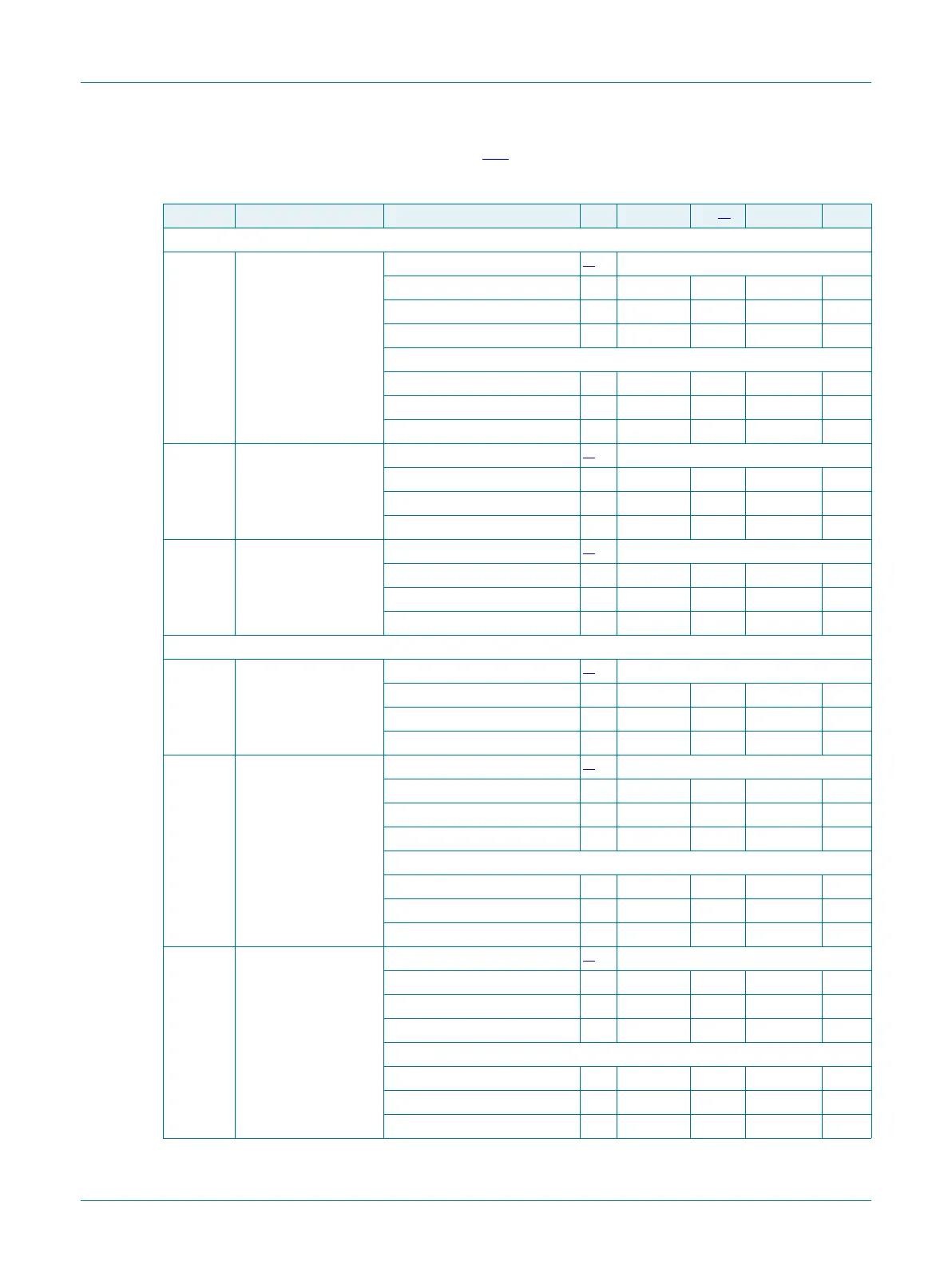
Master; 2.7 V VDD 3.6 V
t
v(Q)
data output valid time on pin I2Sx_TX_SDA
[2]
CCLK = 1 MHz to 12 MHz 24.2 - 40.8 ns
CCLK = 48 MHz to 60 MHz 22.0 - 32.2 ns
CCLK = 96 MHz 21.3 - 30.3 ns
on pin I2Sx_WS
CCLK = 1 MHz to 12 MHz 24.9 - 44.3 ns
CCLK = 48 MHz to 60 MHz 22.6 - 34.0 ns
CCLK = 96 MHz 21.8 - 31.7 ns
t
su(D)
data input set-up time on pin I2Sx_RX_SDA
[2]
CCLK = 1 MHz to 12 MHz 0.0 - - ns
CCLK = 48 MHz to 60 MHz 0.0 - - ns
CCLK = 96 MHz 0.0 - - ns
t
h(D)
data input hold time on pin I2Sx_RX_SDA
[2]
CCLK = 1 MHz to 12 MHz 1.7 - - ns
CCLK = 48 MHz to 60 MHz 1.4 - - ns
CCLK = 96 MHz 1.2 - - ns
Slave; 2.7 V VDD 3.6 V
t
v(Q)
data output valid time on pin I2Sx_TX_SDA
[2]
CCLK = 1 MHz to 12 MHz 17.4 - 33.8 ns
CCLK = 48 MHz to 60 MHz 15.2 - 25.1 ns
CCLK = 96 MHz 14.5 - 23.0 ns
t
su(D)
data input set-up time on pin I2Sx_RX_SDA
[2]
CCLK = 1 MHz to 12 MHz 0.0 - - ns
CCLK = 48 MHz to 60 MHz 0.0 - - ns
CCLK = 96 MHz 0.0 - - ns
on pin I2Sx_RX_WS
CCLK = 1 MHz to 12 MHz 0.0 - - ns
CCLK = 48 MHz to 60 MHz 0.0 - - ns
CCLK = 96 MHz 0.0 - - ns
t
h(D)
data input hold time on pin I2Sx_RX_SDA
[2]
CCLK = 1 MHz to 12 MHz 0.0 - - ns
CCLK = 48 MHz to 60 MHz 0.0 - - ns
CCLK = 96 MHz 0.0 - - ns
on pin I2Sx_RX_WS
CCLK = 1 MHz to 12 MHz 1.0 - - ns
CCLK = 48 MHz to 60 MHz 1.0 - - ns
CCLK = 96 MHz 1.0 - - ns
Table 30. Dynamic characteristics: I
2
S-bus interface pins
[1][4]
T
amb
=
40
C to 105
C; V
DD
= 1.62 V to 3.6 V; C
L
= 30 pF balanced loading on all pins; Input slew = 1.0 ns, SLEW setting =
standard mode for all pins; Parameters sampled at the 90 % and 10 % level of the rising or falling edge.
Symbol Parameter Conditions Min Typ
[3]
Max Unit

 Loading...


