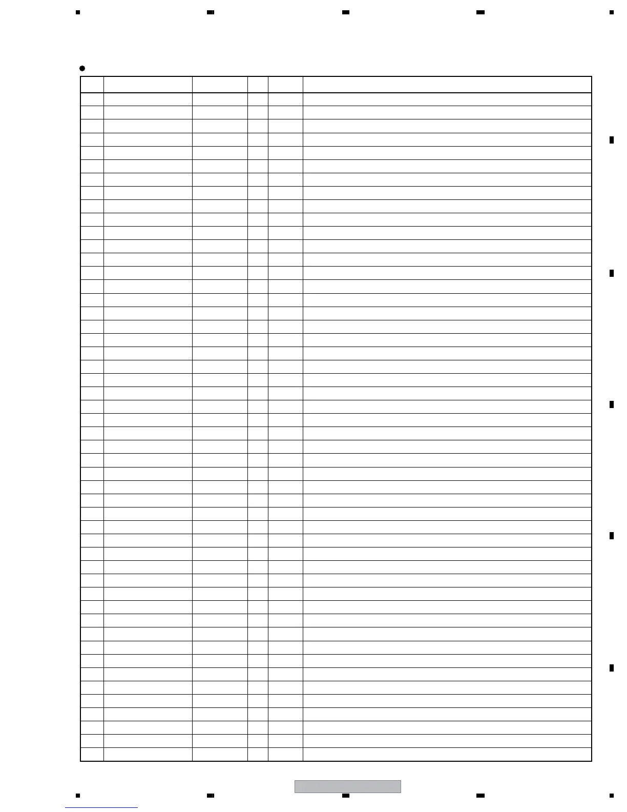
PDP-5000EX
175
5678
56
7
8
C
D
F
A
B
E
Pin Function
No. Mark Pin Name I/O Active Pin Function
1 P94/DA1/TB4IN V_SYNC I L V sync distinction
2 P93/DA0/TB3IN − O
3 P92/TB2IN/SOUT3 TXD_SQ O Serial communication with SQ IC (IC3201 and IC3301) Data transmission
4 P91/TB1IN/SIN3 RXD_AL I
−
Serial communication with SQ IC (IC3201) Data reception
5 P90/TB0IN/VLK3 CLK_SQ O Serial communication with SQ IC (IC3201 and IC3301) Clock output
6 BYTE BYTE I (GND connection)
7 CNVSS CNVSS I For processor mode setting
8 P87/XCIN − O
9 P86/XCOUT − O
10 *RESET RST_MD I L Reset input
11 XOUT XOUT O Output for main clock
12 VSS VSS
−
GND
13 XIN XIN I Input for main clock
14 VCC1 VCC1
−
STB3.3V
15 P85/*NMI NMI I (Pull-up with power)
16 P84/*INT2 − O
17 P83/*INT1 AEM_SQ I H Address emergency input
18 P82/*INT0 RST2 I L Reset detection of SQ IC (IC3201 and IC3301)
19 P81/TA4IN/*U STOP_AR I H Drive stopping monitor of SQ IC (IC3301)
20 P80/TA4OUT/U AR_FUT I H (Reserved) Input for SQ IC (IC3301)
21 P77/TA3IN STOP_AL I H Drive stopping monitor of SQ IC (IC3201)
22 P76/TA3OUT − O
23 P75/TA2IN/*W − O
24 P74/TA2OUT/W − O
25
P73/*CTS2/*RST2/TA1IN/*V
− O
26 P72/CLK2/TA1OUT/V EEPRST O H EEPROM power SW
27
P71/RXD2/SCL2/TA0IN/TB5IN
E_SCL O IIC clock output for EEPROM
28
P70/TXD2/SDA2/TA0OUT
E_SDA I/O IIC data input/output for EEPROM
29 P67/TXD1/SDA1 TXD O Communication with flash ROM writer Data transmission
30 P66/RXD1/SCL1 RXD I Communication with flash ROM writer Data reception
31 P65/CLK1 SCLK I Communication with flash ROM writer Clock input
32
P64/*CTS1/*RTS1/CLKS1
BUSY O Communication with flash ROM writer busy output
33 P63/TXD0/SDA0 RXD_MD O UART communication with main microcomputer Data transmission
34 P62/RXD0/SCL0 TXD_MD I UART communication with main microcomputer Data reception
35 P61/CLK0 AL_FUT I H (Reserved) Input for SQ IC (IC3201)
36 P60/*CTS0/*RTS0 REQ_MD O H Communication request to the main microcomputer
37 P57/*RDY/CLKOUT INP_MUTE O L Output mute of LVDS receiver
38 P56/ALE − O
39 P55/*HOLD EPM I Flash rewriting mode setting (pull-down)
40 P54/*HLDA DRF_B O L High power system OFF
41 P53/BCLK RELAY O H Power ON control
42 P52/*RD
−
O
43 P51/*WRH/*BHE
−
O
44 P50/*WRL/*WR CE I Flash rewriting mode setting (pull-up)
45 P47/*CS3 MODEL I
−
Product distinction (FHD: L)
46 P46/*CS2 SCL O IIC clock output for DAC
47 P45/*CS1 SDA I/O IIC data input/output for DAC
48 P44/*CS0 PD_MUTE_B O L Power down mute
49 P43/A19 LED_B O L Power ON/SD information (For Assy)
50 P42/A18 LED_R O L Power STBY/PD information (For Assy)
 Loading...