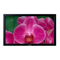
PDP-5000EX
176
1234
1234
C
D
F
A
B
E
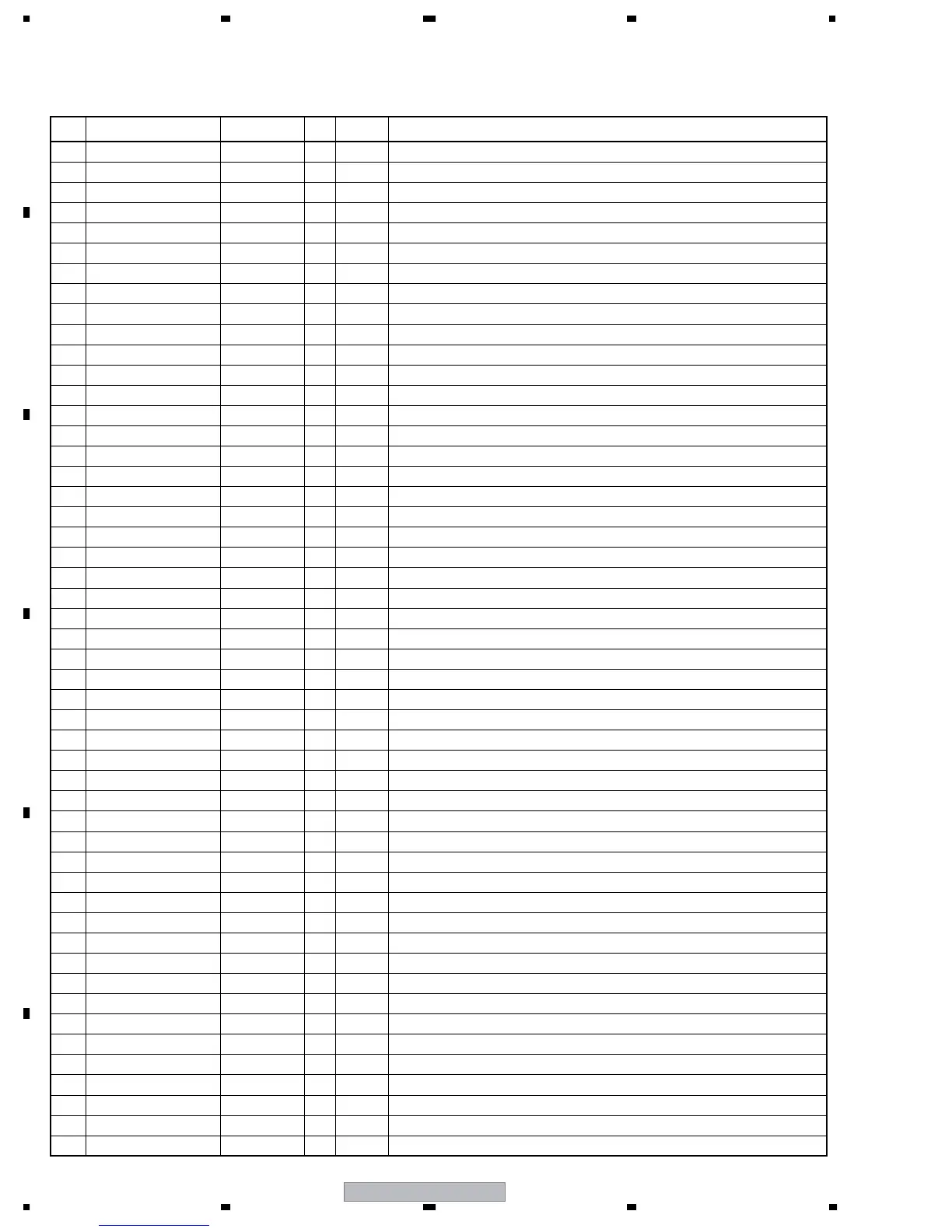
No. Mark Pin Name I/O Active Pin Function
51 P41/A17 H_DET_B I L H existence distinction
52 P40/A16 AL_SEL O H UART switch (For IC3201 selection)
53 P37/A15 RST_SQ O L SQ IC (IC3201 and IC3301) forced reset
54 P36/A14 CE_SQ O L Enable for SQ IC (IC3201 and IC3301) communication
55 P35/A13 BUSY_SQ I H Busy for SQ IC (IC3201 and IC3301) communication
56 P34/A12 − O
57 P33/A11 − O
58 P32/A10 AR_SEL O H UART switch (For IC3301 selection)
59 P31/A9 WE_SQ O H Switching signal of Flash rewriting path for SQ IC
60 VCC2 VCC2 − STB 3.3 V
61 P30/A8(/-/D7) PD_TRG I L EXT_PD confirmation
62 VSS GND − GND
63 P27/AN27/A7(/D7/D6) SCAN_PD I H SCAN decrease voltage PD
64 P26/AN26/A6(/D6/D5) YDRV_PD I H Y drive PD
65 P25/AN25/A5(/D5/D4) YSUS_PD I H Y-SUS PD
66 P24/AN24/A4(/D4/D3) YDCDC_PD I H DCDC converter PD of Y drive
67 P23/AN23/A3(/D3/D2) SCN5V_PD I H SCAN5V decrease voltage PD
68 P22/AN22/A2(/D2/D1) XSUS_PD I H X-SUS PD
69 P21/AN21/A1(/D1/D0) XDCDC_PD I H DCDC converter PD of X drive
70 P20/AN20/A0(/D0/-) XDRV_PD I H X drive PD
71 P17/D15/*INT5 − I
72 P16/D14/*INT4 − I
73 P15/D13/*INT3 AC_DET I L AC power monitor
74 P14/D12 PBF I Panel distinction of High-efficiency/Conventional (FHD: L)
75 P13/D11 − I
76 P12/D10 − I
77 P11/D9 − I
78 P10/D8 − I
79 P07/AN17/D7 ADRS_PD I H Address PD
80 P06/AN16/D6 − I
81 P05/AN15/D5 − I
82 P04/AN14/D4 SS_MODE O L SSCG operation L: SSCG ON, H: SSCG OFF
83 P03/AN13/D3 R_SQ_NON I H Drive stop detection of SQ IC (IC3301)
84 P02/AN12/D2 DDC_PD I H DCDC converter PD
85 P01/AN11/D1 PS_PD I H PD in the POWER SUPPLY Unit
86 P00/AN10/D0 L_SQ_NON I H Drive stop detection of SQ IC (IC3201)
87 P107/AN07/*KI3
OFF_DET_AR
OLDrive stop output to SQ IC (IC3301)
88 P106/AN06/*KI2 DL_FIN_AR I H Rewriting completion signal of SQ IC (IC3301)
89 P105/AN05/*KI1 OFF_DET_AL O L Drive stop output to SQ IC (IC3201)
90 P104/AN04/*KI0 DL_FIN_AL I H Rewriting completion signal of SQ IC (IC3201)
91 P103/AN03 − O
92 P102/AN02 TEMP1 I − Panel temperature sensor input
93 P101/AN01 MODE I − Assy operation mode setting
94 AVSS GND I GND
95 P100/AN00 PSIZE I L G7 size distinction (FHD: L)
96 VREF VREF I − Reference voltage for A/D input
97 AVCC AVCC I STB 3.3 V
98 P97/*ADTRG/SIN4 RXD_AR I L Serial communication with SQ IC (IC3301) Data reception
99 P96/ANEX1/SOUT4 − O
100 P95/ANEX0/CLK4 CLK_SQ I Serial communication with SQ IC (IC3201 and IC3301) Clock input
 Loading...