Copyright © profichip GmbH, 2012
Each receiving device, when addressed, is obliged to generate an
Acknowledge after the reception of each byte. The master device must
generate an extra clock pulse which is associated with this Acknowledge
bit. The device that acknowledges, has to pull down the SDA line during the
acknowledge clock pulse in such a way that the SDA line is stable low
during the high period of the acknowledge related clock pulse. Of course,
setup and hold times must be taken into account. During reads, a master
must signal an end of data to the slave by not generating an Acknowledge
bit on the last byte that has been clocked out of the slave. In this case, the
slave (VPC3+S) will leave the data line high to enable the master to
generate the Stop condition.
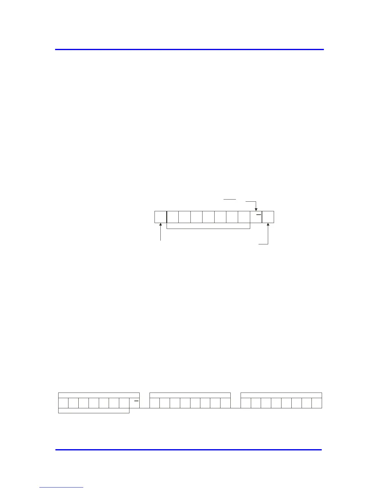
A control byte is the first byte received following the Start condition from the
master device (Figure 8-14). The control byte consists of a seven-bit Slave
Address SA[6:0] to select which device is accessed. The Slave Address
bits in the control byte must correspond to the logic levels on the
I2C_SA[6:0] pins for the VPC3+S to respond.
S
Slave Address
SA6 SA5 SA4 SA3 SA2 SA1 SA0 R/W
START Condition
ACK
Read / BitWrite
Acknowledge Bit
Figure 8-14: Control Byte Format
The last bit of the control byte defines the operation to be performed. When
set to a ‘1’, a read operation is selected. When set to a ‘0’, a write operation
is selected.
The next two bytes received define the address of the first data byte (Figure
8-15). In case of the 4 kB RAM mode is selected only A11 to A0 are used,
the upper four address bits are “don’t care” bits (in case of 2 kB RAM mode
the upper five address bits are “don’t care”).
The upper address bits (MSB) are transferred first, followed by the Less
Significant bits (LSB). Following the Start condition, the VPC3+S monitors
the SDA line checking the control byte transmitted and, upon receiving
appropriate Slave Address bits, the device outputs an Acknowledge signal
on the SDA line. Depending on the state of the R/W bit, the VPC3+S will
select a read or write operation.
Slave Address
SA6 SA5 SA4 SA3 SA2 SA1 SA0 R/WSA6 SA5 SA4 SA3 SA2 SA1 SA0 X X X X A11 A10 A9 A8
Control Byte Address High Byte
A7 A6 A5 A4 A3 A2 A1 A0
Address Low Byte
Figure 8-15: Address Sequence Bit Assignments