R8C/20 Group, R8C/21 Group 14. Timers
Rev.2.00 Aug 27, 2008 Page 217 of 458
REJ09B0250-0200
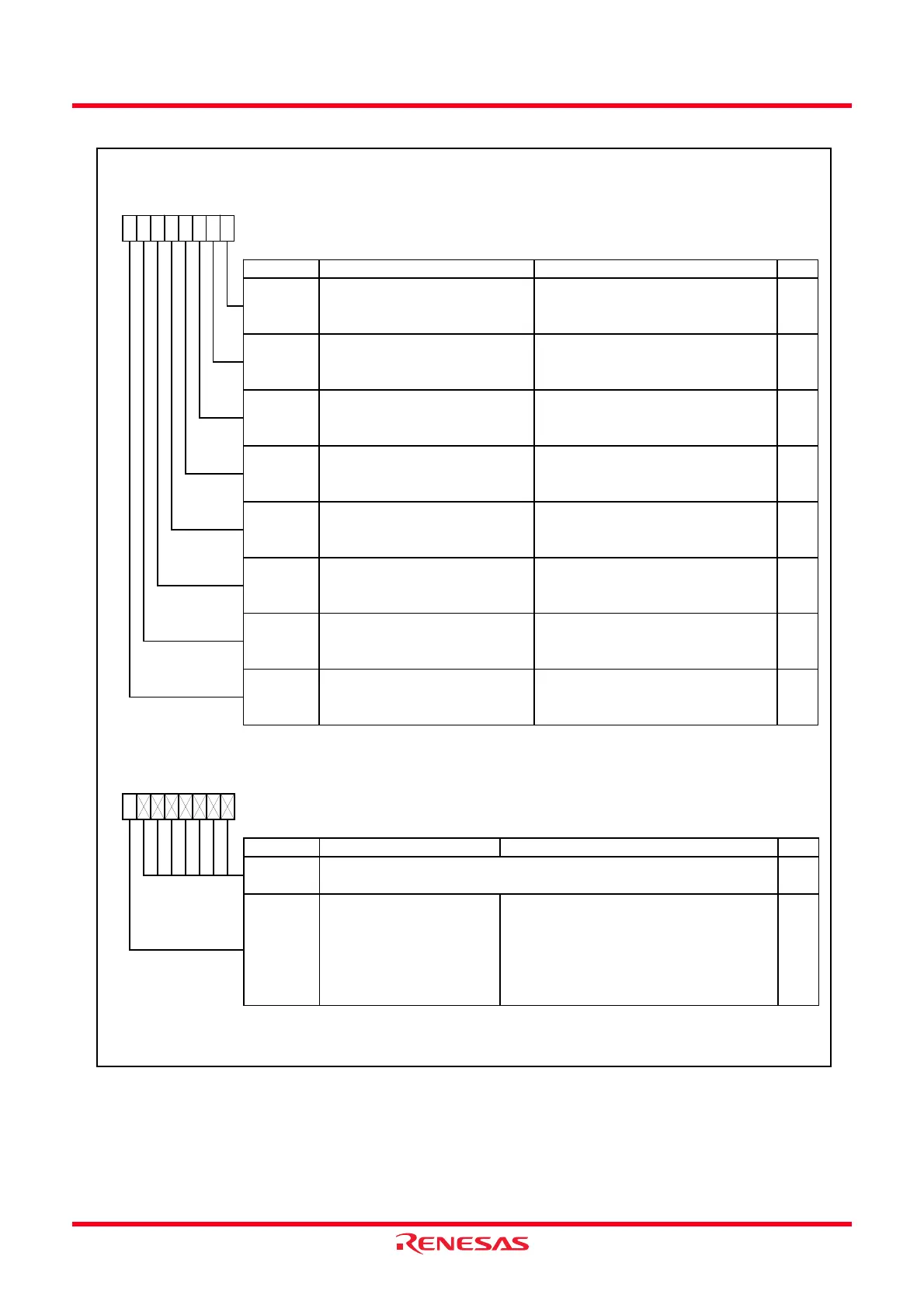
Figure 14.79 Registers TRDOER1 to TRDOER2 in Reset Synchronous PWM Mode
Timer RD Output Master Enable Register 1
Symbol Address After Reset
TRDOER1
013Bh FFh
Bit Symbol Bit Name Function RW
ED1 RW
EA 1
EB1 RW
TRDIOD1 output disable bit 0 : Enable output
1 : Disable output (the TRDIOD1 pin is
used as a programmable I/O port.)
TRDIOB1 output disable bit 0 : Enable output
1 : Disable output (the TRDIOB1 pin is
used as a programmable I/O port.)
EC1
RW
TRDIOA1 output disable bit 0 : Enable output
1 : Disable output (the TRDIOA1 pin is
used as a programmable I/O port.)
RW
RW
TRDIOD0 output disable bit 0 : Enable output
1 : Disable output (the TRDIOD0 pin is
used as a programmable I/O port.)
TRDIOC1 output disable bit 0 : Enable output
1 : Disable output (the TRDIOC1 pin is
used as a programmable I/O port.)
TRDIOC0 output disable bit 0 : Enable output
1 : Disable output (the TRDIOC0 pin is
used as a programmable I/O port.)
EC0 RW
RW
EB0 RW
TRDIOA0 output disable bit Set this bit to 1 (the TRDIOA0 pin is
used as a programmable I/O port) in reset
synchronous PWM mode.
TRDIOB0 output disable bit 0 : Enable output
1 : Disable output (the TRDIOB0 pin is
used as a programmable I/O port.)
b7 b6 b5 b4 b3 b2
ED0
b1 b0
1
EA 0
Timer RD Output Master Enable Register 2
Symbol Address After Reset
TRDOER2
013Ch 01111111b
Bit Symbol Bit Name Function RW
INT0
____
of pulse output forced 0 : Pulse output forced cutoff input disabled
1 : Pulse output forced cutoff input enabled
(all bits in the TRDOER1 register are set to 1
(disable output) w hen “L” is applied to the
INT0
____
pin)
NOTE:
1.
b3 b2 b1 b0b7 b6 b5 b4
Ref er to
14.3.4 Pulse Output Forced Cutoff
.
—
—
(b6 - b0)
Nothing is assigned. If necessary, set to 0.
When read, the content is 1.
RWPTO
cutoff signal input enabled bit
(1)
 Loading...