R8C/20 Group, R8C/21 Group 14. Timers
Rev.2.00 Aug 27, 2008 Page 262 of 458
REJ09B0250-0200
Figure 14.119 TRECSR Register in Output Compare Mode
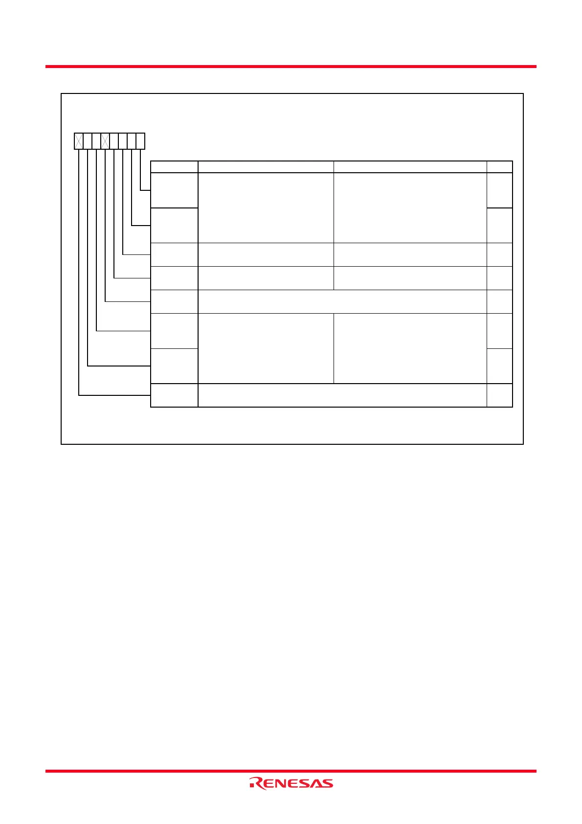
Timer RE Count Source Select Register
Symbol Address After Reset
TRECSR
011Eh 08h
Bit Symbol Bit Name Function RW
NOTE:
1.
b3 b2
—
(b3)
b1 b0
0
RCS0
b7 b6 b5 b4
RW
RCS1 RW
Count source select bit
b1 b0
0 0 : f4
0 1 : f8
1 0 : f32
1 1 : Do not set
4-bit counter select bit 0 : Not used
1 : Used
Write to the RCS5 to RCS6 bits w hen the TOENA bit in the TRECR1 register is set to 0 (disable clock output).
RCS2 RW
RW
—
(b7)
—
Reserved bit Set to 0
Nothing is assigned. If necessary, set to 0.
When read, the content is 0.
—
RW
RCS6 RW
RCS5
—
(b4)
Nothing is assigned. If necessary, set to 0.
When read, the content is 0.
Clock output select bit
(1)
b6 b5
0 0 : f2
0 1 : f4
1 0 : f8
1 1 : Compare output
 Loading...