R8C/20 Group, R8C/21 Group 16. Clock Synchronous Serial Interface
Rev.2.00 Aug 27, 2008 Page 287 of 458
REJ09B0250-0200
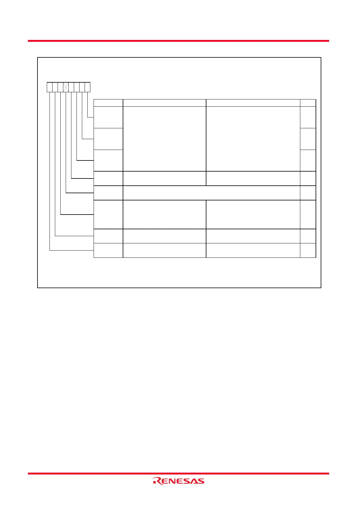
Figure 16.4 SSMR Register
SS Mode Register
Symbol Address After Reset
SSMR
00BAh 00011000b
Bit Symbol Bit Name Function RW
Reserved bit
NOTE:
1.
b3 b2 b1 b0
1
MSB first/LSB first select bit
b7 b6 b5 b4
0 : Change data at odd edge
(dow nloads data at even edge)
1 : Change data at even edge
(dow nloads data at odd edge)
CPOS
SSCK clock polarity select bit
(1)
0 : “H” w hen clock stops
1 : “L” w hen clock stops
—
(b3)
—
(b4)
CPHS
SSCK clock phase select bit
(1)
RO
BC1
BC2
Bit counter 2 to 0
b2 b1 b0
0 0 0 : 8-bit left
0 0 1 : 1-bit left
0 1 0 : 2-bit left
0 1 1 : 3-bit left
1 0 0 : 4-bit left
1 0 1 : 5-bit left
1 1 0 : 6-bit left
1 1 1 : 7-bit left
BC0
RO
RO
Refer to
16.2.1.1 Association between Transfer Clock Polarity, Phase, and Data
for the setting of the CPHS
and CPOS bits.
Set to 1.
When read, its content is 1.
RW
RW
RW
—
RW
0 : Transfers data at MSB first
1 : Transfers data at LSB first
MLS
Nothing is assigned. If necessary, set to 0.
When read, the content is 1.
 Loading...