R8C/20 Group, R8C/21 Group 16. Clock Synchronous Serial Interface
Rev.2.00 Aug 27, 2008 Page 298 of 458
REJ09B0250-0200
16.2.5.2 Data Transmission
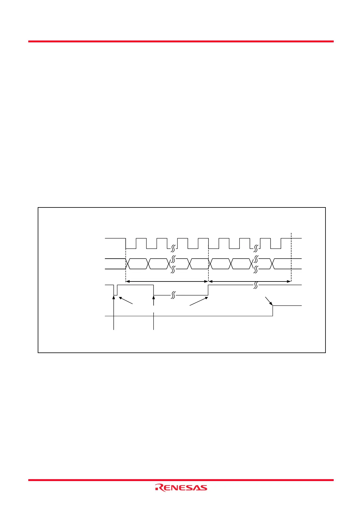
Figure 16.13 shows an Example of Clock Synchronous Serial I/O with Chip Select Operation for Data
Transmission (Clock Synchronous Communication Mode). During the data transmit, the clock synchronous
serial I/O with chip select operates as described below.
When the clock synchronous serial I/O with chip select is set as a master device, it outputs a synchronous clock
and data.
When the clock synchronous serial I/O with chip select is set as a slave device, it outputs data synchronized
with the input clock. When setting the TE bit to 1 (enables transmit) before writing the transmit data to the
SSTDR register, the TDRE bit is automatically set to 0 (data is not transferred from the SSTDR to SSTRSR
registers) and the data is transferred from the SSTDR to SSTRSR registers.
After the TDRE bit is set to 1 (data is transferred from the SSTDR to SSTRSR registers), a transmit is started.
When the TIE bit in the SSER register is set to 1, the TXI interrupt request is generated. When one frame of
data is transferred while the TDRE bit is set to 0, data is transferred from the SSTDR to SSTRSR registers and
a transmit of the next frame is started. If the 8th bit is transmitted while the TDRE bit is set to 1, the TEND bit
in the SSSR register is set to 1 (the TDRE bit is set to 1 when the last bit of the transmit data is transmitted) and
the state is retained. The TEI interrupt request is generated when the TEIE bit in the SSER register is set to 1
(enables transmit-end interrupt request). The SSCK pin is retained “H” after transmit-end.
Transmit can not be performed while the ORER bit in the SSSR register is set to 1 (overrun error occurs).
Confirm that the ORER bit is set to 0 before transmit.
Figure 16.14 shows a Sample Flowchart of Data Transmission (Clock Synchronous Communication Mode).
Figure 16.13 Example of Clock Synchronous Serial I/O with Chip Select Operation for Data
Transmission (Clock Synchronous Communication Mode)
SSCK
b0
SSO
• When SSUMS bit = 0 (clock synchronous communication mode), CPHS bit = 0 (data change
at odd numbers) and CPOS bit = 0 (“H” when clock stops)
b1 b7b0 b1b7
1 frame
TDRE bit in
SSSR register
0
1
TEND bit in
SSSR register
0
1
TEI interrupt request
generation
Write data to SSTDR register
Process by
program
1 frame
TXI interrupt request generation
 Loading...