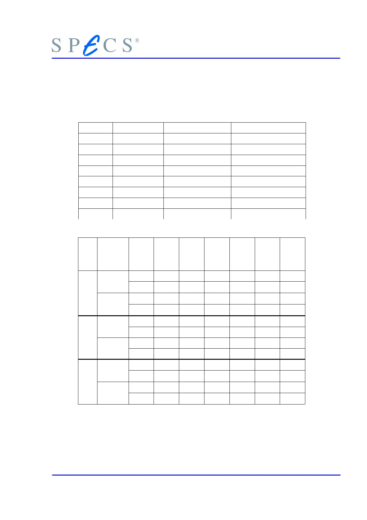
4.2.2 0xe1 – 400V bipolar (HSA3500 module)
Channel ADC name Description DAC Output Pin
0 N / A N / A N / A
1 Mon U0 Voltage Output 0 14
2 Mon I0 Current Output 0 14
3 Mon U1 Voltage Output 1 20
4 Mon I1 Current Output 1 20
5 Mon U2 Voltage Output 2 26
6 Mon I2 Current Output 2 26
7 N / A N / A N / A
Table 28: HSA3500 0xe1 ADC mapping
DAC Voltage
Range
Q5
Fast /
Slow
DAC2
Q4
Fast /
Slow
DAC1
Q3
Fast /
Slow
DAC0
Q2
Range
DAC2
Q1
Range
DAC1
Q0
Range
DAC0
Hex
value
0
-400V to
+400V
1 0x01
1 1 0x09
-40V to
+40V
0x00
1 0x08
1
400V to
+400V
1 0x02
1 1 0x12
-40V to
+40V
0x00
1 0x10
2
400V to
+400V
1 0x04
1 1 0x24
-40V to
+40V
0x00
1 0x20
Table 29: HSA3500 0xe1 Operation Modes
HSA3500 / HSA3500 plus Power Supply 55