For SD card 2 (SDIO2) interface, in order to control independently 1V8_SW, 3V3_SW, and VDDMMC, it is
necessary to control following GPIOs with software:
• SD_LDO_SEL (PG6)
• 3V3_SW_ENABLE (MFX IO0)
• 1V8_SW_ENABLE (MFX IO8)
And the user must follow the hardware configuration described in Table 15.
Table 15. VDDMMC hardware configuration for '1.8V / 3.3V' function (SDIO2)
Signal name Setting
VDDMMC configuration
(1)
OCSPI1_NCS (PG6) JP23 [2-3]
3V3_SW_ENABLE (MFX IO0) SB34
ON
(2)
1V8_SW_ENABLE (MFX IO8) SB29
ON
(2)
1. The default setting is in bold.
2. PB8 signal is supplied by VDDMMC. Make sure to supply 3.3V on VDDMMC (Refer to Section 6.3.5 ).
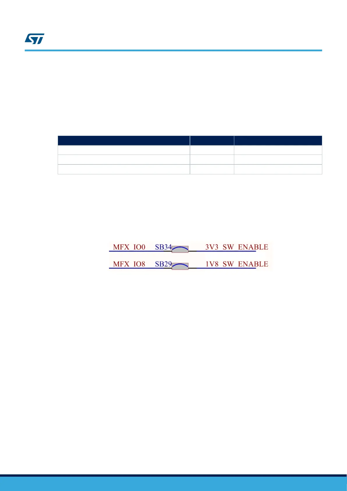
Make sure to take into account schematics below (Figure 18, Figure 19, Figure 20, and Figure 21).
• DNF means that the component is not fitted by default on the board.
Schematics for 3V3_SW, 1V8_SW, and VDDMMC
Figure 18. 3V3_SW_SW_ENABLE and 1V8_SW_ENABLE MFX schematic (Page 2)
UM2662
Power supply
UM2662 - Rev 1
page 25/95