6 Hardware layout and configuration
The STM32H7B3I-EVAL Evaluation board is designed around the STM32H7B3LIH6QU target microcontroller.
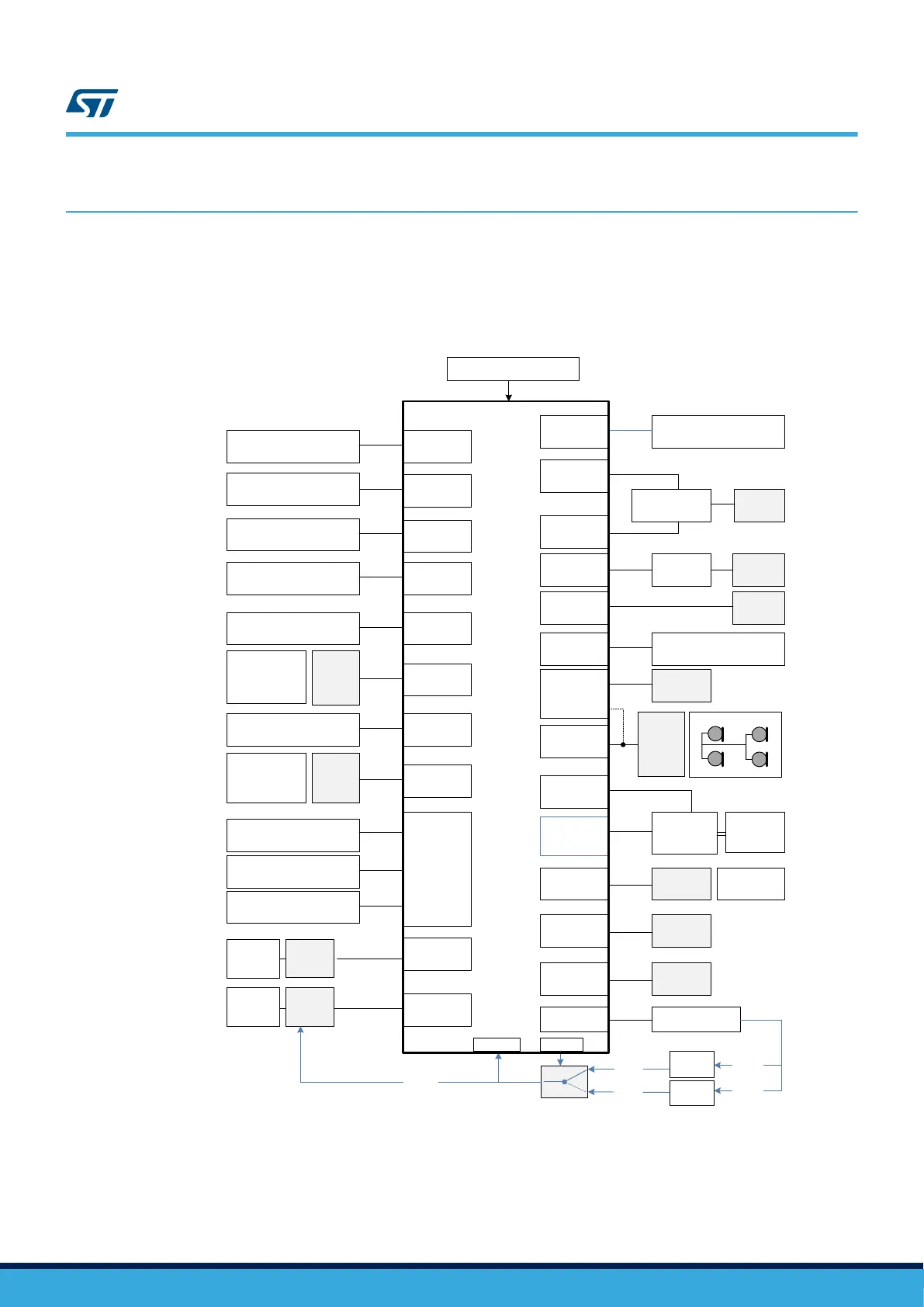
Figure 2 illustrates STM32H7B3LIH6QU connections with peripheral components.
Figure 2. Hardware block diagram
3V3 Power Supply
(3V3_AO)
LED, push-button, and wake-up
External USB
HS PHY
MIcro-AB
USB
connector
Wi-Fi
®
module
GPIOs
OTG HS (ULPI)
OTG FS
UART + SPI +
GPIOs
VCP UART
SWD
VBAT
LSE
LCD
Reset
FMC
SDIO 1
SDIO 2
I2C
SAI1 or I2S6
and / or
differential ADC
GPIO, I
2
C, INT
Audio codec
CS42L51-CNZ
3 V battery
32 KHz crystal
RK070ER9427L
RGB - 7 INCH –
WVGA
LCD + CTP
MB1370 module
8 Mx32bit SDRAM
8 Mx16bit NOR Flash
microSD
TM
card 2.0
(3V3)
microSD
TM
card 3.0
(3V3 / 1V8)
STM32L152CCT6
MFX GPIO Expander
Stereo jack
(line-out)
STM32F723IEK6
STLINK V3.0
Micro-B
USB
connector
MB1299 Module
1 Mx16bit SRAM
HSE
24 MHz crystal
Reset button
OCSPI 2
OCSPI
connector
OCSPI 1
MX25LM51245GXDI00
OCSPI
DFSDM1 and 2
DFSDM
ADC Potentiometer
ADCs, PWMs,
GPIOs,
DFSDM
Motor-control
connector
CAN, CAN FD,
and bootloader
RS-232
DB9
connectors
GPIOs
Extension
connectors
DCMI
Camera
module
connector
DFSDM
connector
MB1242
OCSPI module
microSD
TM
card
connector
3V3_SW
LDO
3V3_SW
MB1379
camera module
Micro-AB
USB
connector
LCD +
CTP
connector
STM32H7B3LIH6QU
VDDMMC
MFX IO0
VDDMMC
1V8_SW
LDO
1V8_SW
GPIO
MFX IO8
ON/OFF
ON/OFF
SEL
microSD
TM
card
connector
Note: Interfaces in blue are partially supplied by VDDMMC. Refer to Section 6.3.5 .
UM2662
Hardware layout and configuration
UM2662 - Rev 1
page 7/95