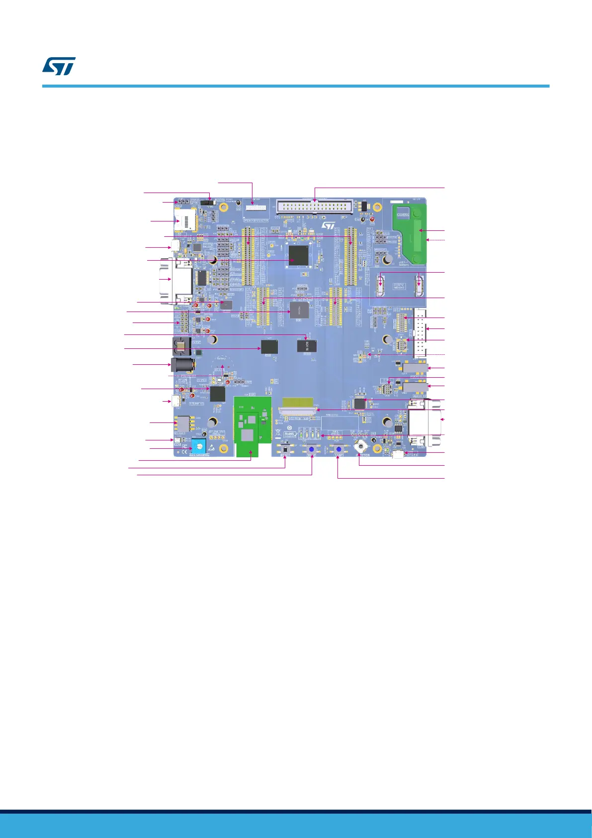
Figure 3 shows the location of the main components on the top side of the Evaluation board.
Figure 3. STM32H7B3I-EVAL Evaluation board layout
CN9: UART RS-232 connector
CN3: microSD™ connector
CN8: USB HS connector
JP29: 5 V selection
CN17: 5 V DC jack
CN21: ST-LINK USB connector
U21: MCU STLINK-V3
CN24: EXT I
2
C connector
LD9: ST-LINK COM LED
CN12/CN13: Extension connectors
U11: Octo-SPI Flash
CN5/CN6: Extension connectors
RV1: ADC potentiometer
U12: NOR Flash
U16: SDRAM
U17: SRAM
JPME1: Power meter connector
U5: STM32H7B3LIH6QU
U24: Wi-Fi
®
module
SW1: BOOT0 switch
CN4: MB1299 DFSDM microphones module connector
B1: Reset button
B2: Wake-up button
CN10/CN11: MB1242 Octo-SPI module connector
CN2: MB1379 camera module connector
CN1: Motor-control connector
CN28: microSD™ connector (bottom)
CN15: ETM trace connector
CN14: JTAG connector
CN16: MIPI-10 connector
U48: Audio codec (bottom)
CN18: Audio stereo output jack
CN20: Audio stereo input jack
CN22: CANFD connector
U25: I/O expander
CN23: MB1370 LCD module RGB connector
CN30: MB1370 LCD module CTP connector
LD1/LD2/LD3/LD4: User LEDs
CN27: USB FS connector
B4: Joystick
B3: Tamper button
CN29: Battery connector (bottom)
UM2662
Hardware layout and configuration
UM2662 - Rev 1
page 8/95