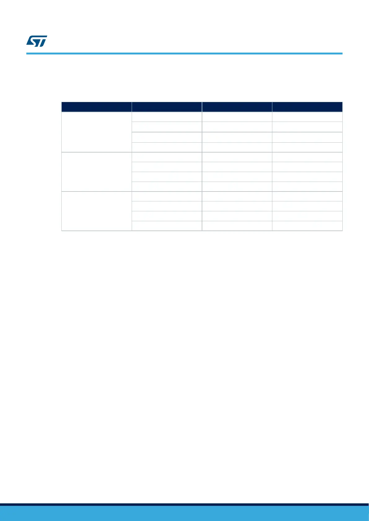
Hardware modifications are listed in Table 49 below:
Table 49. Configuration for SRAM A19-A22 (Just for the test)
Pin name Signal name Setting NOR
PE3
SAI1_SD_B JP34 OFF
WIFI_SPI4_NSS R337
OFF
(1)
TRACED0 R93
OFF
(1)
FMC_A19 R97 ON just for test
PE4
SAI1_FS_A JP26 N/A
TRACED1 R340 N/A
DCMI_D4 R116 N/A
FMC_A20 R88 ON just for test
PE5
WIFI_SPI4_MISO R69 N/A
SAI1_SCK_A JP28 N/A
TRACED2 R71 N/A
FMC_A21 R324 ON just for test
1. Remove to avoid stub if necessary.
Note: If using SD card 1 (Default configuration), use FMC_NE3 = PG10, then SD card 2 cannot be used). If using SD
card 2, use FMC_NE3 = PC8 by fitting JP12 [2-3], then SD card 1 cannot be used.
8.3
microSD™ card 2
8.3.1 Description
A microSD
™
card connector connected to the SDIO2 3.0 port of STM32H7B3LIH6QU is available on the board.
The microSD
™
card detection is managed by SD_DETECT2 (PI11).
It supports SD 3.0, SDR104, SDR50, DDR50, SDR25, SDR12 and SD 2.0 high-speed (50 MHz) and default
speed (25 MHz) modes.
SDIO2 signals are all supplied by VDDMMC. Make sure to supply 3.3 V or 1.8 V on VDDMMC (Refer to Section
6.3.5 ).
8.3.2 Operating voltage
As SDIO2 is in the VDDMMC domain (VDDMMC = 3.3 V or 1.8 V), when going to UHS1 mode (1.8 V), the
STG4160 switch U2 allows switching signals from 3.3 V to 1.8 V using the SD_LDO_SEL signal (PG6). 3V3_SW
and 1V8_SW can also be switched OFF using MFX IO0 and MFX IO8 in case a power-off sequence is needed.
8.3.3 Limitations and hardware configuration
Limitations with primary functions: camera and OCSPI1 (Refer to jumper configuration below)
Limitations with secondary functions: SRAM and OCSPI2
UM2662
microSD™ card 2
UM2662 - Rev 1
page 54/95