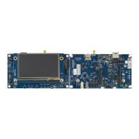
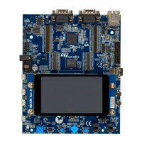
Hardware modifications are listed in Table 32:
Table 32. Hardware configuration for SDRAM
Pin name Signal name Setting
SDRAM
(1)
PF0
FMC_A0 R339 ON
OCSPI2_IO0 R98
OFF
(2)
PF1
FMC_A1 R335 ON
OCSPI2_IO1 R89
OFF
(2)
PF2
FMC_A2 R331 ON
OCSPI2_IO2 R82
OFF
(2)
PF3
FMC_A3 R74 ON
OCSPI2_IO3 R75
OFF
(2)
PG0
FMC_A10 R73 ON
OCSPI2_IO4 R76
OFF
(2)
PG1
FMC_A11 R333 ON
OCSPI2_IO5 R77
OFF
(2)
PF4
FMC_A4 R66 ON
OCSPI2_CLK R319
OFF
(2)
PF5
FMC_A5 R65 ON
OCSPI2_NCLK R318
OFF
(2)
PG15
FMC_SDNCAS R352 ON
OCSPI2_DQS R354
OFF
(2)
1. The default setting is in bold.
2. Remove to avoid stub if necessary.
7.7
Octo-SPI NOR Flash 1
7.7.1 Description
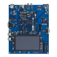
One 512-Mbit Octo-SPI NOR Flash Macronix MX25LM51245GXDI00 is connected to OCSPI1 interface of
STM32H7B3LIH6QU on the STM32H7B3I-EVAL Evaluation board.
7.7.2 Operating voltage
STM32H7B3LIH6QU OCSPI1 interface can only be at 3.3 V on this board. Make sure to supply 3.3 V on
VDDMMC (Refer to Section 6.3.5 ).
7.7.3 Limitations and hardware configuration
Limitations with secondary function: SDIO2.
UM2662
Octo-SPI NOR Flash 1
UM2662 - Rev 1
page 38/95
 Loading...
