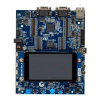
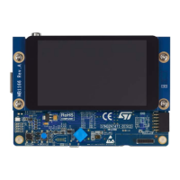
Hardware modifications are listed in Table 33:
Table 33. OCSPI1 hardware configuration
Signal name Pin name Setting
OCSPI1
(1)
OCSPI1_IO6 / SDIO2_CK
PD6
(2)
JP4 [1-2]
OCSPI1_NCS / SD_LDO_SEL PG6 JP23 [1-2]
3V3_SW_ENABLE
MFX IO0
(2)
SB34 ON
1. The default setting is in bold.
2. PD6 signal is supplied by VDDMMC. Make sure to set MFX_IO0 to 1 in order to supply 3.3V on VDDMMC (Refer to Section
6.3.5 )
7.8 Analog input
7.8.1 Description
The two-pin header CN7 and 10 KΩ potentiometer RV1 are connected to PA0_C of STM32H7B3LIH6QU as an
analog input. A low-pass filter can be implemented by replacing R221 and C96 with the right value of resistor and
capacitor as requested by the end user’s application.
7.8.2 Operating voltage
The STM32H7B3LIH6QU analog input interface can only be at 3.3 V on this board.
7.8.3 Interface
Figure 27. Analog I/O connector CN7
12
Table 34. Analog I/O connector CN7 pinout
Pin number Description Pin number Description
1 Analog I/O (PA0_C) 2 GND
UM2662
Analog input
UM2662 - Rev 1
page 39/95
 Loading...