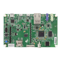
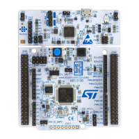
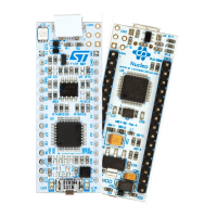
Hardware modifications are listed in Table 47 below:
Table 47. Configuration for SRAM A19 (Just for the test)
Pin name Signal name Setting SRAM
PE3
SAI1_SD_B JP34 OFF
WIFI_SPI4_NSS R337
OFF
(1)
TRACED0 R93
OFF
(1)
FMC_A19 R97 ON just for test
1. Remove to avoid stub if necessary.
Note: If using SD card 1 (Default configuration), use FMC_NE3 = PG10, then SD card 2 cannot be used). If using SD
card 2, use FMC_NE3 = PC8 by fitting JP12 [2-3], then SD card 1 cannot be used.
8.2 NOR
8.2.1 Description
128Mbit NOR Flash Micron MT28EW128ABA1LPC-0SIT is connected to bank1 NOR/PSRAM1 of the FMC
interface. The 16-bit operation mode is selected by a pull-up resistor connected to the BYTE pin of the NOR Flash
memory.
8.2.2 Operating voltage
STM32H7B3LIH6QU FMC interface (SDRAM, SRAM, and NOR) can only be at 3.3 V on this board.
8.2.3 Limitations and hardware configuration
The write protection can be enabled by fitting jumper JP25.
Limitations with primary functions: camera and DFSDM (Refer to jumper configuration Table 48 below)
Limitations with secondary functions: OCSPI2 FMC addresses
UM2662
NOR
UM2662 - Rev 1
page 52/95
 Loading...
