6.4.2 Reset source
The reset signal of STM32H7B3I-EVAL Evaluation board is active low and the reset sources include:
• Reset button B1
• Debugging tools from JTAG/SWD connector CN14 and ETM trace connector CN15
• Daughterboard from CN6
• Embedded STLINK-V3E
• RS-232 connector CN9 for ISP
Note: The jumper JP24 must be closed for RESET handling with pin8 of RS-232 connector CN9 (CTS signal).
6.4.3 Boot option
The STM32H7B3I-EVAL Evaluation board can boot from:
• Embedded user Flash memory
• System memory with a bootloader for ISP
• Embedded SRAM for debugging
The boot option is configured by setting switch SW1 (BOOT) and the boot base address programmed in the
BOOT_ADD0 and BOOT_ADD1 option bytes. The BOOT can be configured also via RS-232 connector CN9.
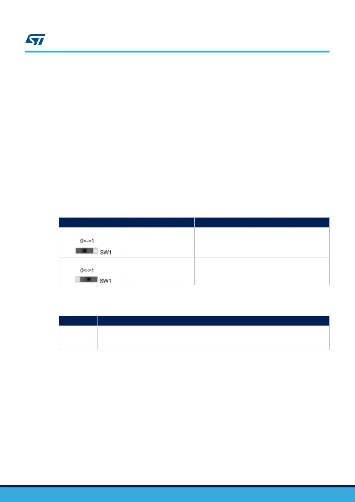
Table 18. Boot related switch
Switch configuration Boot address option bytes
Boot space
(1)
0
BOOT_ADD0[15:0]
Boot address defined by user option byte
BOOT_ADD0[15:0]
ST programmed value:
Flash memory at 0x0800 0000
1
BOOT_ADD1[15:0]
Boot address defined by user option byte BOOT_ADD1[15:0]
ST programmed value:
System bootloader at 0x1FF0 0000
1. The default setting is in bold.
Table 19. Boot related jumpers
Jumper
Description
(1)
JP22
OFF
The Bootloader_BOOT0 is managed by pin 6 of connector CN9 (RS-232 DSR signal) when JP22 is ON.
This configuration is used for bootloader application only.
1. The default setting is in bold.
6.5
VCP ST-LINK UART
6.5.1 Description
Virtual COM port (VCP) UART can be connected to MCU pins PB14/PB15 (Default configuration) or PA2/PA3
(Compatible with bootloader).
UART to USB conversion is done by STLINK-V3E STM32F723IEK6 MCU U21 and routed to USB debug
connector CN21.
6.5.2 Operating voltage
The STM32H7B3LIH6QU UART interface can only be at 3.3 V on this board.
UM2662
VCP ST-LINK UART
UM2662 - Rev 1
page 28/95