Hardware modifications are listed in Table 50 below:
Table 50. Configuration for NOR A0-A5, A10-11 addresses, and command
Signal name Setting
SDIO2 configuration
(1)
SDIO2_D0 (PG9) (DCMI_VSYNC) JP17
[2-3]
(2)
SDIO2_D1 (PG10)
R118
OFF
(3)
R115
OFF
(3)
R280
ON
(2)
JP2
[2-3]
(2)
SDIO2_D2 (PG11) (DCMI_D3)
R257 OFF
JP1
[2-3]
(2)
SDIO2_D3 (PG12) R122
ON
(2)
SD_LDO_SEL (PG6) (OCSPI1_NCS) JP23
[2-3]
(2)
SDIO2_CK (PD6) JP4
[2-3]
(2)
SD_DETECT2 (PI11) JP13
ON
(2)
3V3_SW_ENABLE (MFX IO0) SB34
ON
(2)
1V8_SW_ENABLE (MFX IO8) SB29
ON
(2)
1. The default configuration is in bold.
2. SDIO2 signals are all supplied by VDDMMC. Make sure to supply 3.3 V or 1.8 V on VDDMMC (Refer to Section 6.3.5 ).
3. Remove to avoid stub if necessary.
Note: Remove the MB1242 OCSPI module when using the SD card 2 interface.
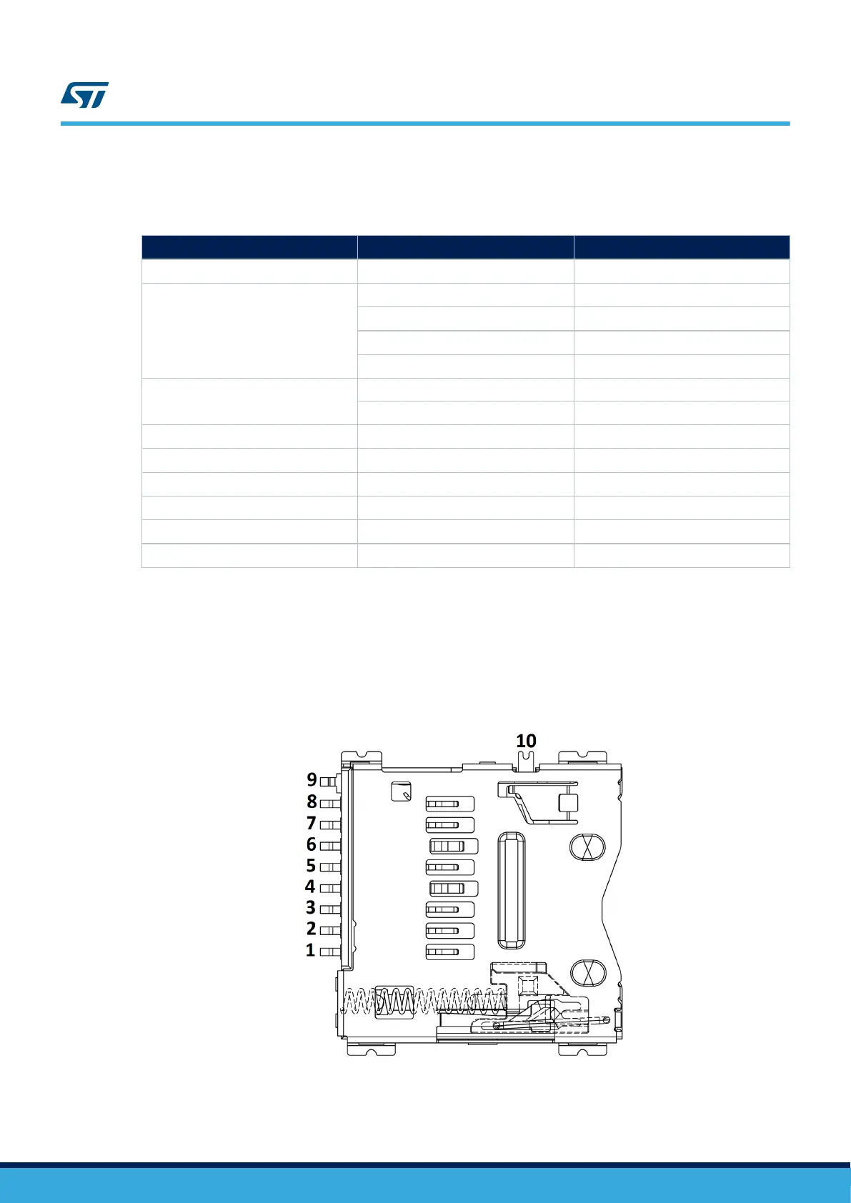
8.3.4 Interface
Figure 31. microSD
™
connector CN3
UM2662
microSD™ card 2
UM2662 - Rev 1
page 55/95