Address register (I2CADDR)
Address comparator
Data shift register (I2CDATA)
ACK SDA
Arbitration and synchronization logic
SCL
Serial clock generator
System
clock
Control register (I2CCFG)
Interrupt
Control
logic
P2
interrupt
Status register (I2CSTAT)
XDATA Bus
Operation
www.ti.com
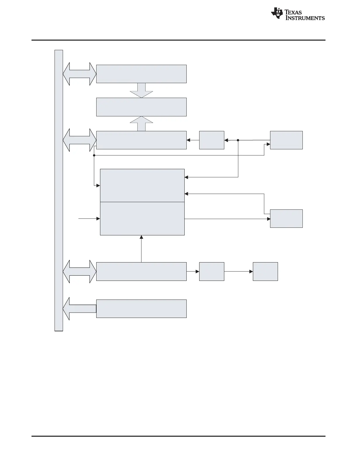
Figure 20-1. Block Diagram of the I
2
C Module
20.1 Operation
The I
2
C module supports any slave or master I
2
C-compatible device. Figure 20-2 shows an example of an
I
2
C bus. Each I
2
C device is recognized by a unique address and can operate as either a transmitter or a
receiver. A device connected to the I
2
C bus can be considered as the master or the slave when
performing data transfers. A master initiates a data transfer and generates the clock signal, SCL. Any
device addressed by a master is considered a slave.
I
2
C data is communicated using the serial data (SDA) pin and the serial clock (SCL) pin. Both SDA and
SCL are bidirectional and must be connected to a positive supply voltage using a pullup resistor.
178
SWRU191C–April 2009–Revised January 2012
I
2
C
Submit Documentation Feedback
Copyright © 2009–2012, Texas Instruments Incorporated