www.ti.com
General-Purpose I/O DMA
When an interrupt condition occurs on one of the I/O pins, the interrupt status flag in the corresponding
P0–P2 interrupt flag register, P0IFG, P1IFG, or P2IFG, is set to 1. The interrupt status flag is set
regardless of whether the pin has its interrupt enable set. When an interrupt is serviced, the interrupt
status flag is cleared by writing a 0 to that flag. This flag must be cleared prior to clearing the CPU port
interrupt flag (PxIF).
The SFR registers used for interrupts are described later in this section. The registers are summarized as
follows:
• P0IEN: P0 interrupt enables
• P1IEN: P1 interrupt enables
• P2IEN: P2 interrupt enables
• PICTL: P0, P1, and P2 edge configuration
• P0IFG: P0 interrupt flags
• P1IFG: P1 interrupt flags
• P2IFG: P2 interrupt flags
7.5 General-Purpose I/O DMA
When used as general-purpose I/O pins, the P0 and P1 ports are each associated with one DMA trigger.
These DMA triggers are IOC_0 for P0 and IOC_1 for P1, as shown in Table 8-1.
The IOC_0 trigger is activated when an interrupt occurs on the P0 pins. The IOC_1 trigger is activated
when an interrupt occurs on the P1 pins.
7.6 Peripheral I/O
This section describes how the digital I/O pins are configured as peripheral I/Os. For each peripheral unit
that can interface with an external system through the digital input/output pins, a description of how
peripheral I/Os are configured is given in the following subsections.
For USART and timer I/O, setting the appropriate PxSEL bits to 1 is required for the output signals on a
digital I/O pin to be controlled by the peripheral. For peripheral inputs from digital I/O pins, this is optional.
PxSEL = 1 overrides the pullup/pulldown settings of a pin, so to be able to control pullup/pulldown with
the PxINP bits, the PxSEL bit should be set to 0 for that pin.
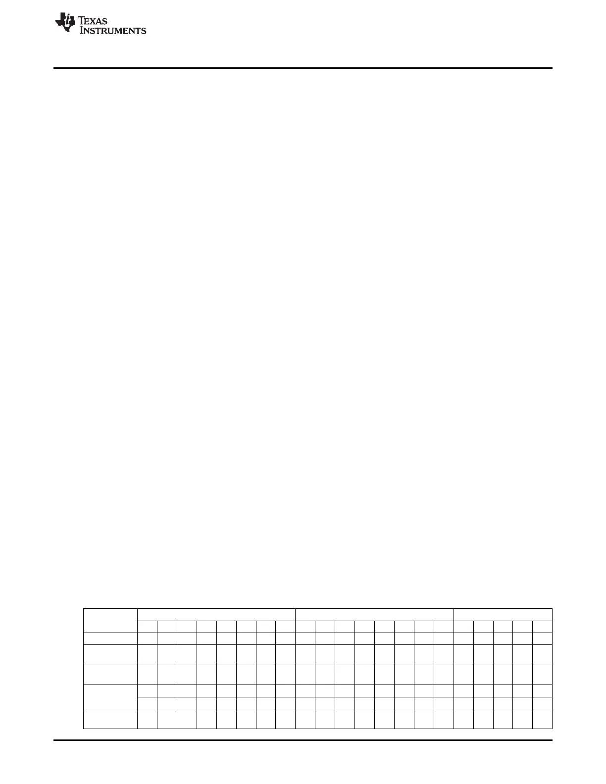
Note that peripheral units have two alternative locations for their I/O pins; see Table 7-1. Priority can be
set between peripherals if conflicting settings regarding I/O mapping are present (using the
P2SEL.PRIxP1 and P2DIR.PRIP0 bits). All combinations not causing conflicts can be used.
Note that a peripheral normally is present at the selected location even if it is not used, and another
peripheral that is to use the pins must be given higher priority. The exception is the RTS and CTS pins of
a USART in UART mode with flow control disabled and the SSN pin of a USART configured in SPI master
mode.
Note also that peripheral units that have input pins receive an input from the pin regardless of the PxINP
setting, and this may influence on the state of the peripheral unit. For instance, a UART should be flushed
before use if there may have been activity on the RX pin prior to taking it in use as a UART pin.
Table 7-1. Peripheral I/O Pin Mapping
P0 P1 P2
Periphery/
Function
7 6 5 4 3 2 1 0 7 6 5 4 3 2 1 0 4 3 2 1 0
ADC A7 A6 A5 A4 A3 A2 A1 A0 T
Operational
O – +
amplifier
Analog
+ –
comparator
USART 0 SPI C SS MO MI
Alt. 2 M0 MI C SS
USART 0
RT CT TX RX
UART
83
SWRU191C–April 2009–Revised January 2012 I/O Ports
Submit Documentation Feedback
Copyright © 2009–2012, Texas Instruments Incorporated