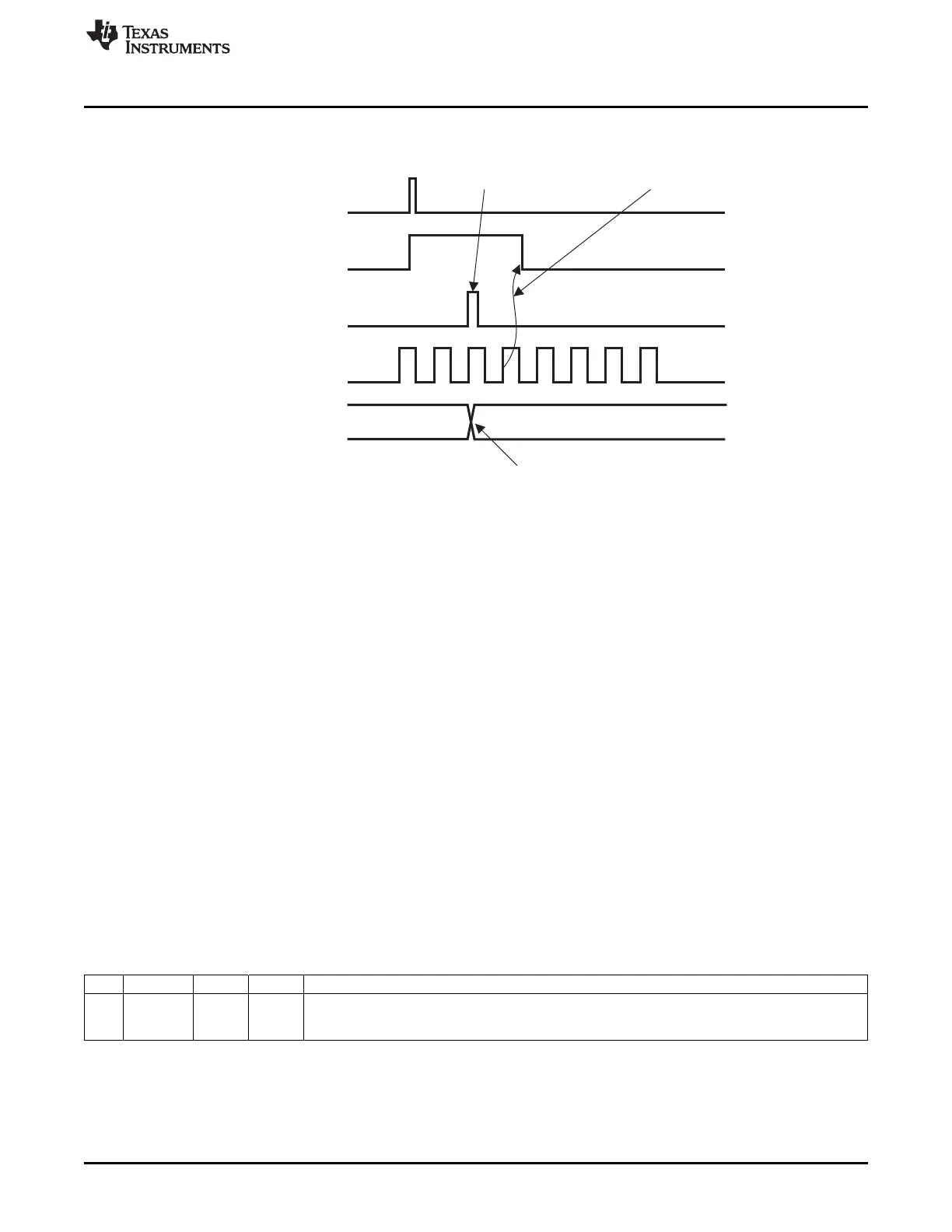
P0_0
P0IFG[0]
STCS.VALID
SLEEPSTA.CLK32K
STCV[23:0]
Read STCV[23:0],
ThenClear
STCS.VALID
Clear P0IFG[0] After
HavingDetecteda
RisingEdgeOn
SLEEPSTA.CLK32K
TimerValueisCaptured
T0412-01
www.ti.com
Sleep Timer Registers
Figure 11-1. Sleep Timer Capture (Example Using Rising Edge on P0_0)
It is not possible to switch the input-capture pin while capture is enabled. Capture must be disabled before
a new input-capture pin can be selected. To disable capture, follow these steps (note that interrupts will be
disabled for up to half of a 32-kHz cycle, or 15.26 µs):
1. Disable interrupts.
2. Wait until SLEEPSTA.CLK32K is high.
3. Set STCC.PORT[1:0] to 3. This disables capture.
11.4 Sleep Timer Registers
The registers used by the Sleep Timer are:
• ST2 – Sleep Timer 2
• ST1 – Sleep Timer 1
• ST0 – Sleep Timer 0
• STLOAD – Sleep Timer load status
• STCC – Sleep Timer capture control
• STCS – Sleep Timer capture status
• STCV0 – Sleep Timer capture value byte 0
• STCV1 – Sleep Timer capture value byte 1
• STCV2 – Sleep Timer capture value byte 2
ST2 (0x97) – Sleep Timer 2
Bit Name Reset R/W Description
7:0
ST2[7:0]
0x00 R/W Sleep Timer count/compare value. When read, this register returns the high bits [23:16] of the Sleep
Timer count. When writing, this register sets the high bits [23:16] of the compare value. The value
read is latched at the time of reading register ST0. The value written is latched when ST0 is written.
135
SWRU191C–April 2009–Revised January 2012 Sleep Timer
Submit Documentation Feedback
Copyright © 2009–2012, Texas Instruments Incorporated