CC253x
CC2541
V
CC
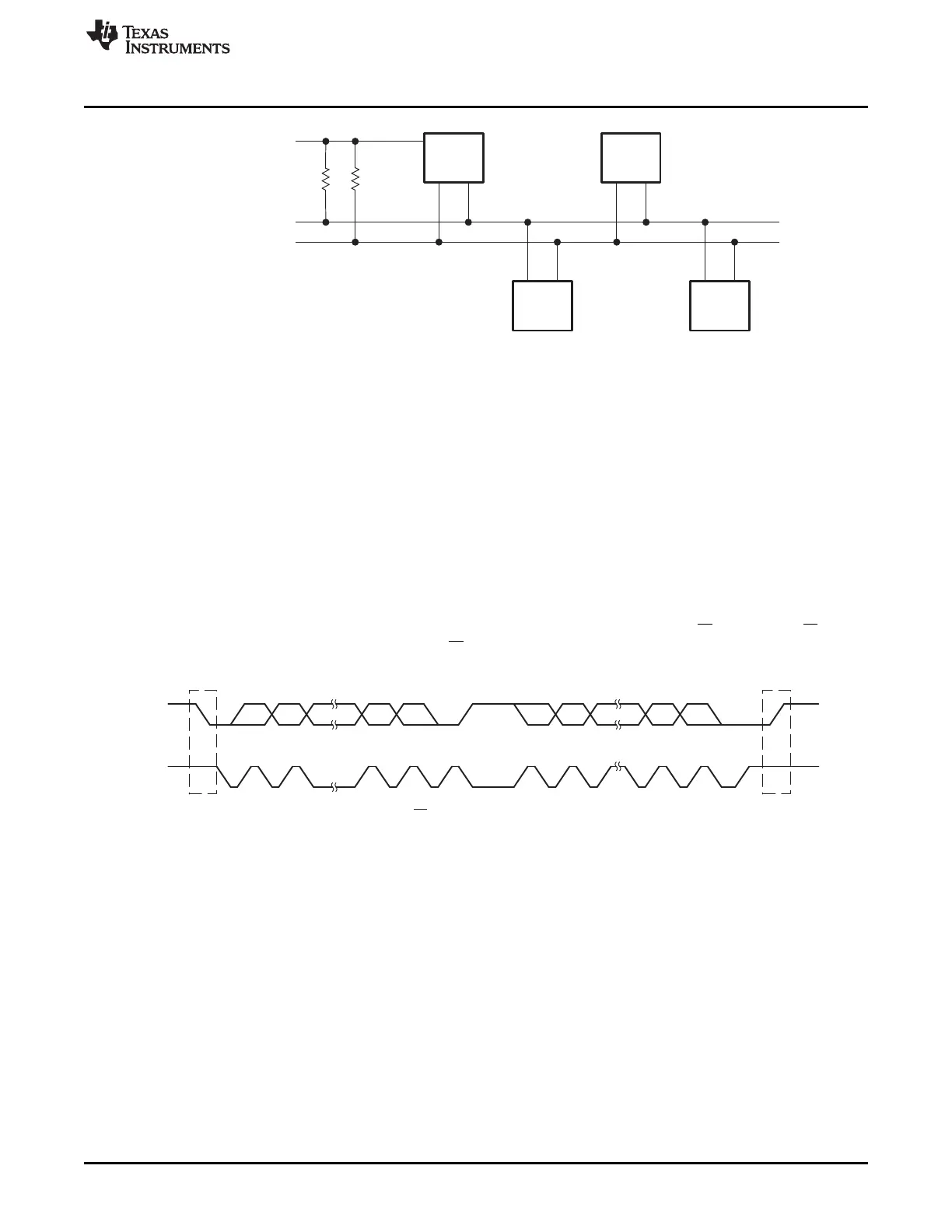
Serial Data (SDA)
Serial Clock (SCL)
Device A
Device B
Device C
SDA
SCL
MSB Acknowledgement
Signal From Receiver
Acknowledgement
Signal From Receiver
1 2 7 8 9 1 2 8 9
ACK ACK
START
Condition (S)
STOP
Condition (P)
R/W
www.ti.com
Operation
Figure 20-2. I
2
C Bus Connection Diagram
20.1.1 I
2
C Initialization and Reset
The I
2
C module is enabled by setting the I2CCFG.ENS1 bit. It is then in the not-addressed slave state.
The I
2
C configuration and state is not retained in power modes PM2 and PM3. It must be reconfigured
after coming out of sleep mode.
The I
2
C module is not reset when disabled, and retains its internal state until the next time I2CCFG.ENS1
is set.
20.1.2 I
2
C Serial Data
One clock pulse is generated by the master device for each data bit transferred. The I
2
C module operates
with byte data. Data is transferred MSB first as shown in Figure 20-3.
The first byte after a START condition consists of a 7-bit slave address and the R/W bit. When R/W = 0,
the master transmits data to a slave. When R/W = 1, the master receives data from a slave. The ACK bit
is sent from the receiver after each byte on the ninth SCL clock.
Figure 20-3. I
2
C Module Data Transfer
START and STOP conditions are generated by the master and are shown in Figure 20-3. A START
condition is a high-to-low transition on the SDA line while SCL is high. A STOP condition is a low-to-high
transition on the SDA line while SCL is high.
Data on SDA must be stable during the high period of SCL (see Figure 20-4). The state of SDA can only
change when SCL is low, otherwise a START or STOP condition is generated.
179
SWRU191C–April 2009–Revised January 2012
I
2
C
Submit Documentation Feedback
Copyright © 2009–2012, Texas Instruments Incorporated