166
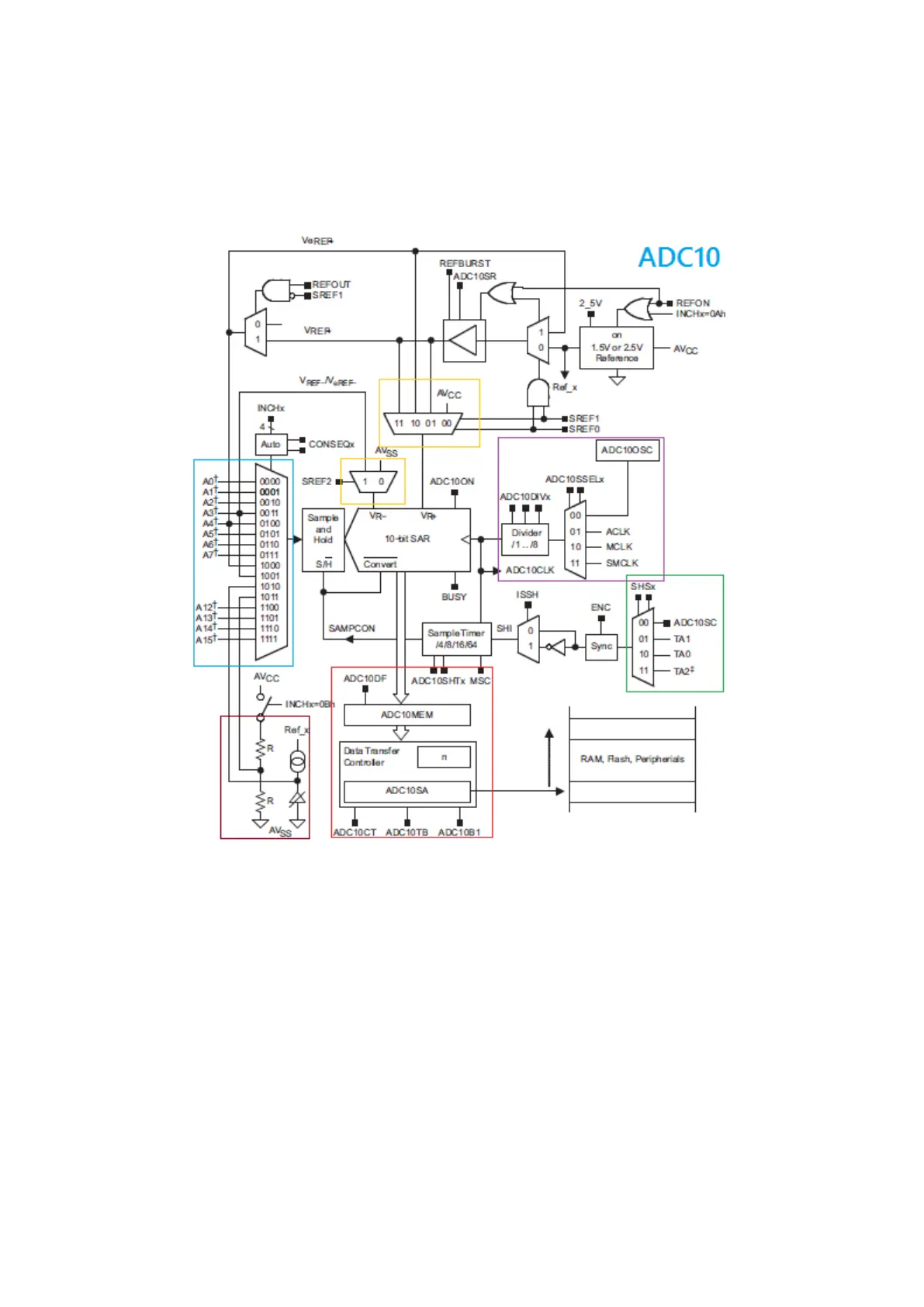
ADC10
In most value-line devices (VLD) like MSP430G2553 and MSP430G2452, ADC12 is not present and the
ADC tasks are accomplished with ADC10 modules.
Shown above is the simple block diagram of the ADC10 module. ADC10 is a SAR ADC. Highlighted
segments include:
• ADC channel selector (light blue area) – select the highest channel from where the first ADC
conversion starts. An internal counter counts down from this channel all the way down to A0.
• DMA and ADC output (red area) – here we get AD conversion results and can optionally do a
peripheral to memory DMA transfer.
• ADC clock source (purple area) – this is the clock source that runs the ADC.
• ADC trigger source (light green area) – selects what triggers the ADC to start a conversion.
• Reference selectors (orange boxes) – selects ADC’s positive and negative references.
• Built-in signal sources (Deep red area) – includes on-chip temperature sensor, supply voltage
sensing voltage divider, etc.