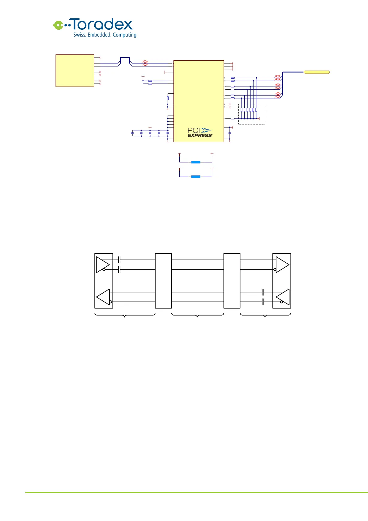
Figure 4: PCIe reference clock buffer example
2.2.2.1 PCIe x1 Slot Connector Schematic Example
For a regular PCIe slot connector, no additional decoupling capacitors are permitted to be placed
on the carrier board in the RX, TX and reference clock lines. The decoupling capacitors are located
on the module and the PCIe card.
Figure 5: PCIe x1 Slot Connector Block Diagram
The Verdin module standard features a dedicated PCIe reset. This reset (PCIE_1_RESET#) should be
used to guarantee the power ramp up timing requirements of PCI Express. Since the PCIe slot
connector has a 3.3V logic level and the PCIE_1_RESET# output of the module is only 1.8V, a level
shifter is required. Please note that the Verdin module standard does not support PCIe hot-plug
functionality.
The PCIe x1 slot connector has two card present signals (PRSNT1#, pin A1 and PRSNT2#, pin B18)
which are shorted to ground by the card (if it is inserted). Since the Verdin standard does not
feature the PCIe hot-plug feature, these pins can be left unconnected or connected to any free
module GPIOs if the presence detection of the card needs to be emulated.
The wake output of the PCIe slot (WAKE#, pin B11) can be connected to the general wake input of
the Verdin module (CTRL_WAKE1_MICO#). Wake-up-capable PCIe cards such as Ethernet cards
can use this signal to wake up the module from the suspend state. The WAKE# signal of the PCIe
card slot is an open drain type. Therefore, no level shifter is required if the signal is pulled up to
1.8V on the carrier board, and not to 3.3V.
The JTAG interface on the PCIe slot can be left unconnected. This interface is only used for
debugging purposes. No termination on the carrier board is needed.