The PCIe slot pin-out features an SMB interface for additional power management control. As the
SMB and I2C buses are compatible from a hardware perspective, it is recommended that the
general purpose I2C_1 interface of the Verdin module is used if the SMB interface is needed. Most
PCIe cards do not make use of the SMB interface though. Therefore, these pins can be left
unconnected for most applications. Please note that the SMB interface has a logic level of 3.3V
while the I2C_1 has 1.8V. Therefore, a bidirectional level shifter is required.
According to the PCIe specifications, the regular +3.3V supply rail (pin A9, A10, and B8) as well as
the +12V (pin A2, A3, B1 and B2) are required to be provided. The +3.3Vaux is optional.
However, the +3.3Vaux must be supplied to the PCIe add-in card slot if the platform supports the
wake features (WAKE#).
Not all PCIe cards need the +12V supply. For a battery powered system or a carrier board with a
wide voltage input range, it might be difficult to generate a regulated 12V rail. In this case, we
recommend checking with the PCIe card(s) manufacturer to determine if the +12V supply is
required. Please note that omitting the +12V is violating the PCI Express specifications and makes
therefore the design incompatible with some add-in cards.
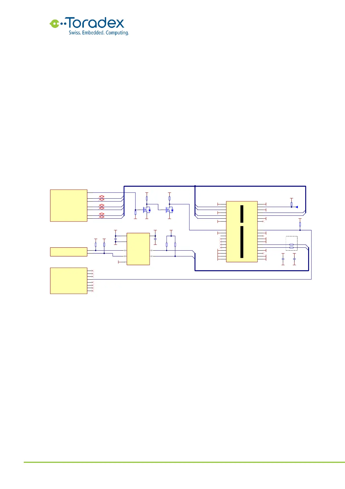
Figure 6: PCIe x1 slot reference schematic
2.2.2.2 Mini PCIe Card Schematic Example
The Mini PCIe Card (also called PCI Express Mini Card, Mini PCI Express or Mini PCIe) features
beside the PCIe link an USB 2.0 high-speed interface. In order to be compliant, the carrier board
needs to provide both interfaces, the PCIe and USB. As most of the Mini PCIe Cards use only one
of its interfaces for an embedded carrier board which is developed for a restricted set of
compatible cards, it might be enough to implement only the required interface. Check with the
Mini PCIe Card vendor whether the USB, PCIe or both interfaces are used by the card.
The Mini PCIe Card features the decoupling capacitors for the RX lines on the card. Therefore, no
additional decoupling capacitors should be placed on the carrier board in either the RX, TX or
reference clock lines.