ZED-F9P-Integration Manual
UBX-18010802 - R02
5 Hardware description Page 69 of 114
Advance Information
5 Hardware description
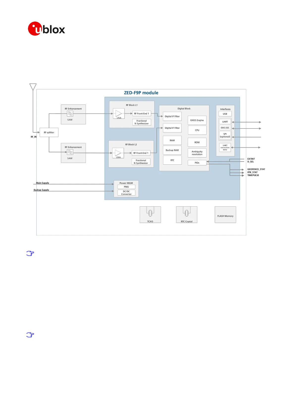
5.1 Block diagram
Figure 43: ZED-F9P block diagram
An active antenna is mandatory with the ZED-F9P.
5.2 Connecting power
The u-blox ZED-F9P module has two power supply pins: VCC, V_BCKP.
5.2.1 VCC: Main supply voltage
The VCC pin provides the main supply voltage. During operation, the current drawn by the module
can vary by some orders of magnitude. For this reason, it is important that the supply circuitry be
able to support the peak power for a short time (see the u-blox u-blox ZED-F9P Data sheet [1] for
specification).
The module integrates a DC/DC converter, which allows reduced power consumption.
When switching from backup mode to normal operation or at start-up, u-blox ZED-F9P
modules must charge the internal capacitors in the core domain. In certain situations, this
can result in a significant current draw. For low power applications using backup mode, it is
important that the power supply or low ESR capacitors at the module input can deliver this
current/charge.
 Loading...