ZED-F9P-Integration Manual
UBX-18010802 - R02
8 Design Page 83 of 114
Advance Information
8 Design
This section details the required information to carry out a schematic and PCB design.
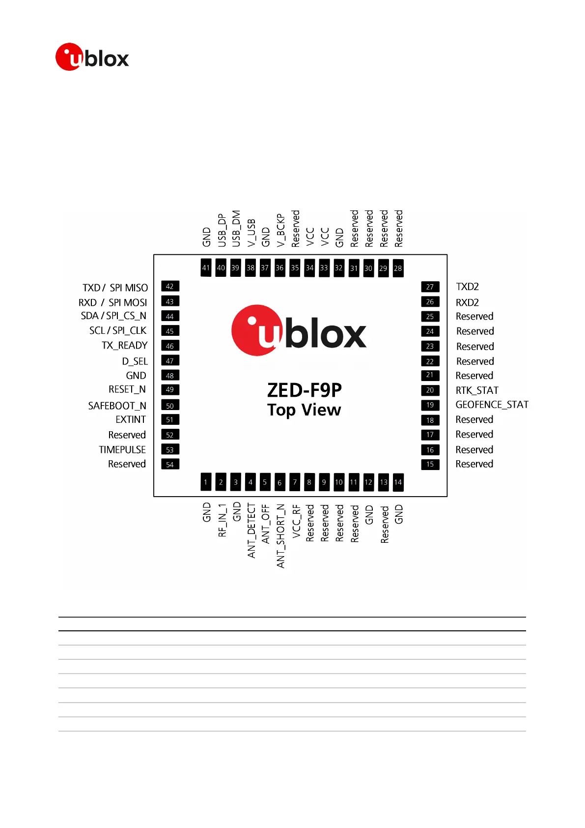
8.1 Pin assignment
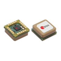
The pin assignment of the ZED-F9P module is shown in Figure 54. The defined configuration of the
PIOs is listed in Table 22.
Figure 54: ZED-F9P pin assignment
Pin No Name I/O Description
1 GND - Ground
2 RF_IN_1 I RF input
3 GND - Ground
4 ANT_DETECT I Active antenna detect - default active high
5 ANT_OFF O External LNA disable - default active high
6 ANT_SHORT_N I Active antenna short detect - default active low
7 VCC_RF O Voltage for external LNA
 Loading...