ZED-F9P-Integration Manual
UBX-18010802 - R02
8 Design Page 93 of 114
Advance Information
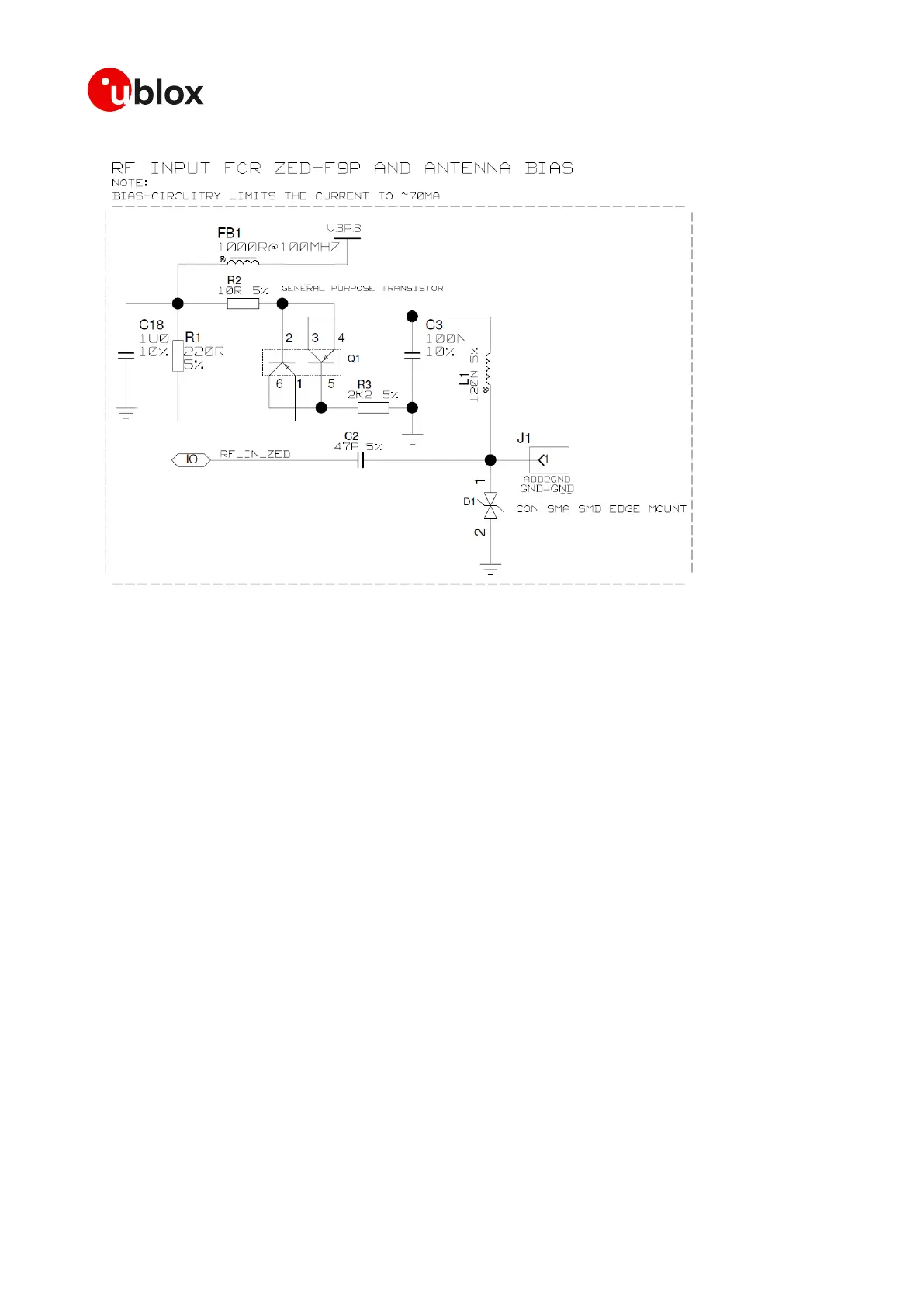
Figure 68: ZED-F9P antenna bias
L1: MURATA LQW15A 0402 120N 5% 0.11A -55/+125C
D1: TYCO, 0.25PF, PESD0402-140 -55/+125C
C2: MURATA GRM0335C1H470JA01 47pF ±5% 50Vdc C0G(EIA) 0±30ppm -55 to 125C
C3: MURATA GRM155R61A104KA01 CER X5R 0402 100N 10% 10V
8.7 Layout
This section details layout and placement requirements of the ZED-F9P high precision receiver.
8.7.1 Placement
GNSS signals at the surface of the Earth are about 19 dB below the thermal noise floor. A very
important factor in achieving maximum GNSS performance is the placement of the receiver on
the PCB. The Placement used may affect RF signal loss from antenna to receiver input and enable
interference into the sensitive parts of the receiver chain, including the antenna itself. When
defining a GNSS receiver layout, the placement of the antenna with respect to the receiver, as well
as grounding, shielding and interference from other digital devices are crucial issues and need to
be considered very carefully.
Signal loss on the RF connection from antenna to receiver input must be minimized as much as
possible. Hence, the connection to the antenna must be kept as short as possible.
Make sure that RF critical circuits are clearly separated from any other digital circuits on the system
board. To achieve this, position the receiver digital part towards your digital section of the system
PCB and have the RF section and antenna placed as far as possible away from the other digital
circuits on the board.
A proper GND concept shall be followed: The RF section should not be subject to noisy digital supply
currents running through its GND plane.
 Loading...