English
INSTALLATIONANDCONNECTION
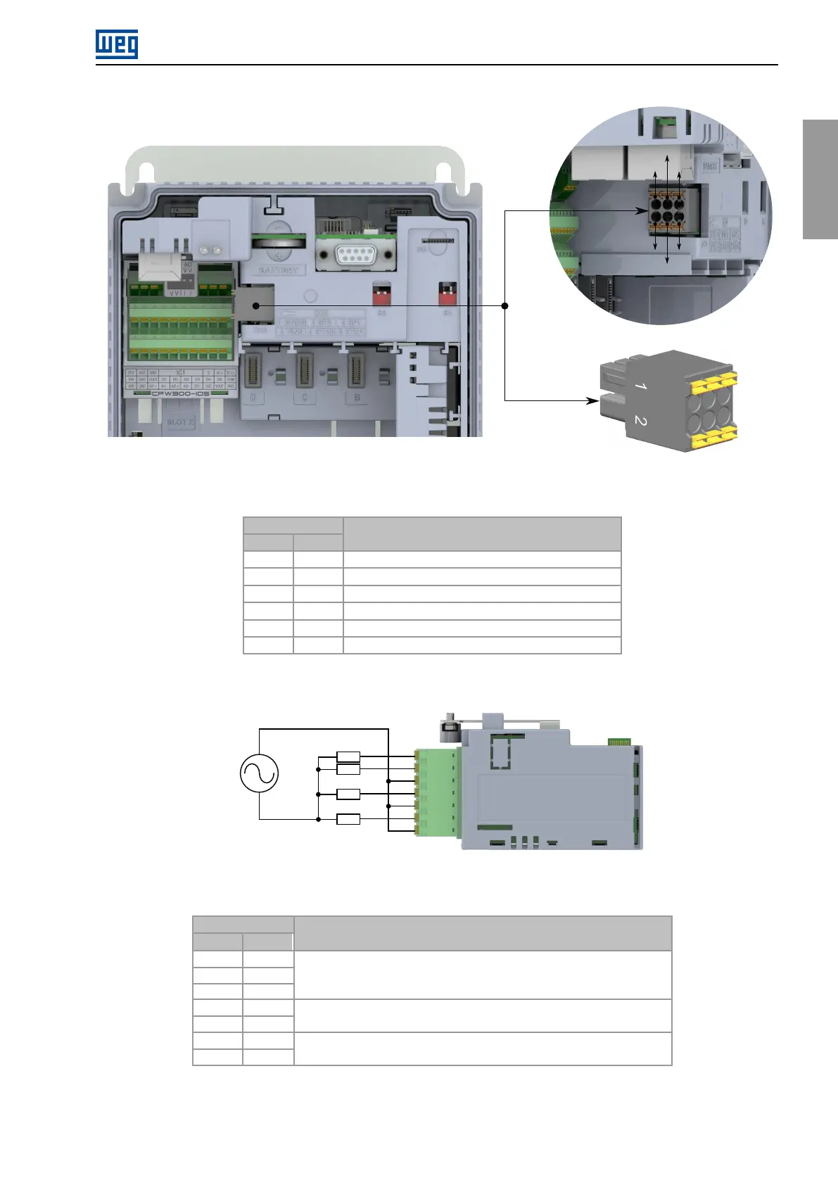
Indication of pins 1 e 2
GNDS
2
4
6
1
2
3
4
5
6
SP2
SP1
VINS
STO2
STO1
1
3
5
Figure3.21:XC2connectorlocationandpinout
Table3.13:XC2connector(safetymodule)
XC2connector
PinName
Description:
(1)
1GNDS
Safetymodulereference
2VINS
+24Vdcpowersupplyforthesafetymodule
3SP2
SafetysignalforSTO2input
4STO2
Safetyinput2
5SP1
SafetysignalforSTO1input
6STO1
Safetyinput1
(1)
Formoreinformationandconnectionexamples,refertotheCFW900safety
manual.
NF1
NA1
C1
NA2
C2
NA3
C3
F
N
1
2
3
4
5
6
7
Figure3.22:CFW900-REL-01XC30connectorpinoutwithexampleofACloadconnection
Table3.14:XC30connector(CFW900-REL-01Accessory)
XC30connector
PinName
Description:DefaultFunction(ifany)
(1)
1NF1
1ADigitalRelayOutput:Nofault
(2)
NO:NormallyOpen,C:Common,NC:
Normallyclosed
2NA1
3C1
4NA2
2ADigitalRelayOutput:
(2)
N>Nx(S2.1.1>C5.9.4)
5C2
6NA3
3ADigitalRelayOutput
(2)
N*>Nx(S2.1.3>C5.9.4)
7C3
(1)
FormoreinformationseethedetailedspecificationinTable8.13.
(2)
TheCFW900-REL-01suppliedwiththeinverterwillbeconnectedtoslotA,andthe
correspondingoutputswillbe1A,2Aand3A,withthedefaultfunctionsindicated.Iftheaccessory
isreconnectedtoanotherslot,theidentificationoftheoutputswillchangeto1n,2nand3n,with
‘n’beingtheslotwheretheaccessorywasconnected.
CFW900|41