7 Series FPGAs GTP Transceivers User Guide www.xilinx.com 133
UG482 (v1.9) December 19, 2016
RX Out-of-Band Signaling
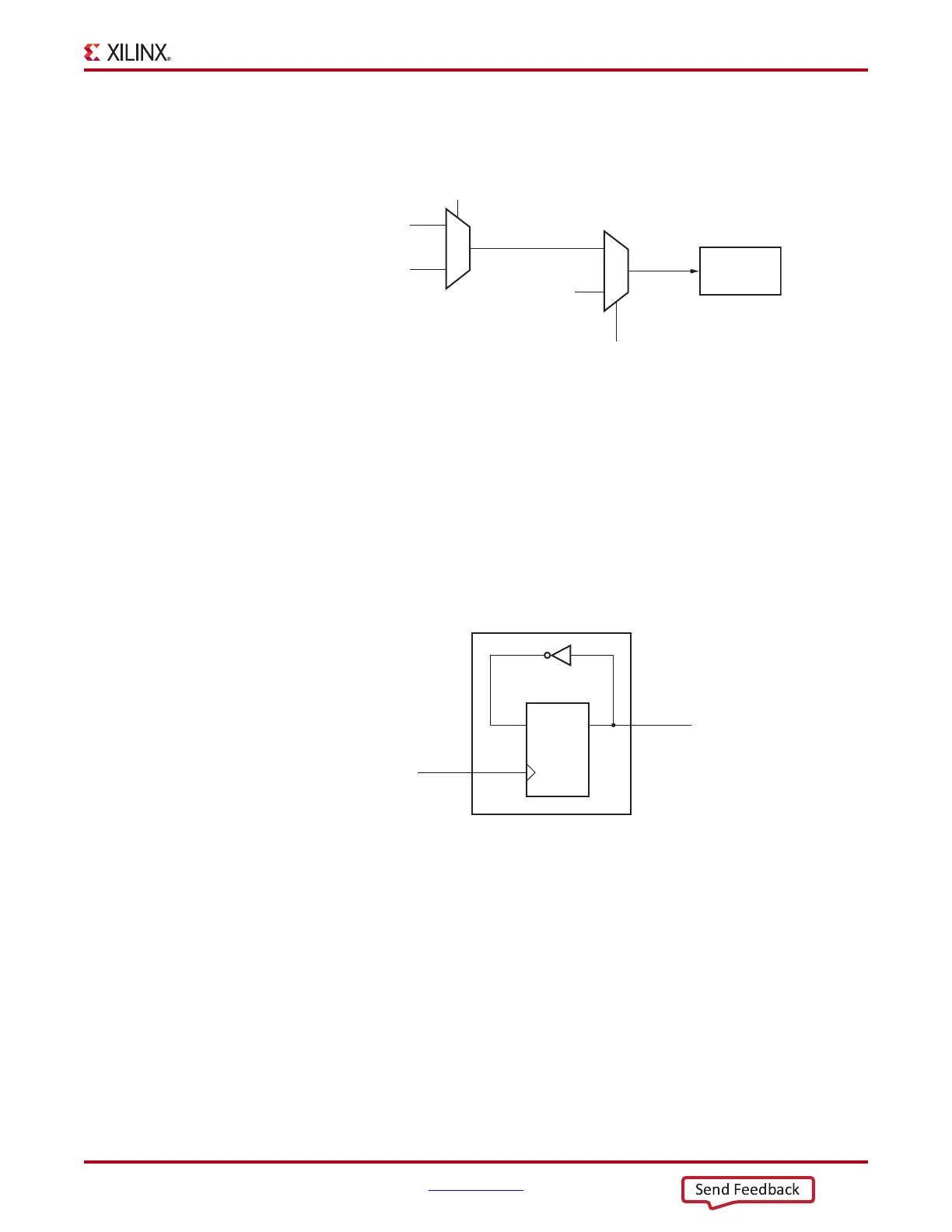
Also, the attribute PCS_RSVD_ATTR[8] should be set to 1'b1. The OOB circuit has two possible
sources from which it can receive a clock, as shown in Figure 4-6.
The attribute RXOOB_CLK_CFG controls the source of oobclk. Setting RXOOB_CLK_CFG to
1'b0 selects the reference clock connected to PLL0 or PLL1. RXSYSCLKSEL controls which of
the two reference clocks is selected. Setting RXOOB_CLK_CFG to 1'b0 selects an alternative
clock source from SIGVALIDCLK. A divided down reference clock can be connected to the
SIGVALIDCLK port pin, providing an alternative clock for the OOB circuit.
The divided down clock(s) requires no special phase relationships between other clocks in the
SERDES. However, there is a requirement of a 50% duty cycle. Figure 4-7 and Figure 4-8 show the
method for clock division. Figure 4-7 shows how a simple toggle flip-flop can be used to divide the
REFCLK.
X-Ref Target - Figure 4-6
Figure 4-6: Clocking Mechanism for the OOB Detect Circuit
X-Ref Target - Figure 4-7
Figure 4-7: Toggle Flip-Flop to Divide REFCLK
RXSYSCLKSEL
SIGVALIDCLK
PLL0REFCLK
PLL1REFCLK
RXOOB_CLK_CFG
OOB
UG482_c4_106_021113
(Port)
0
1
0
1
RXPLLREFCLK_DIV1
oobclk
(Port)
(Attribute)
Clk
Input
Q
Clk/2
Output
D
UG476_c4_107_071712