134 www.xilinx.com 7 Series FPGAs GTP Transceivers User Guide
UG482 (v1.9) December 19, 2016
Chapter 4: Receiver
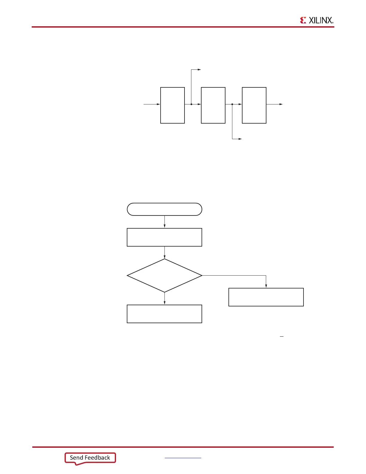
Figure 4-8 shows how cascading several divide-by-two circuits produces higher order clock
dividers such as divide-by-4 and divide-by-8.
Use Modes
For OOB operating at a line rate of 1.5 Gb/s or below, see the flowchart in Figure 4-9 to determine
the frequency f of the OOB clock.
The requirement in Equation 4-1 must be satisfied for the OOB to work correctly.
Equation 4-1
OOB operating at line rates > 1.5 Gb/s is an advanced feature. Operation for certain protocols at
higher line rates such as PCIe (Gen1 and Gen2) and SATA are addressed in Table 4-8.
X-Ref Target - Figure 4-8
Figure 4-8: Clock Dividers
div2 div2 div2 Clk/8
Clk/2
Clk/4
Clk
UG482_c4_108_020413
X-Ref Target - Figure 4-9
Figure 4-9: Flowchart for Protocols with Line Rates < 1.5G
f ≤ Linerate / (3 x Runlength)
RX is in Electrical Idle
RX is Not in Electrical Idle
Is RXELECIDLE
Asserted?
No
Ye s
For Linerate ≤ 1.5 Gb/s
UG482_c4_109_0020413
f linerate 3 runlength×()⁄≤