7 Series FPGAs GTP Transceivers User Guide www.xilinx.com 15
UG482 (v1.9) December 19, 2016
Overview and Features
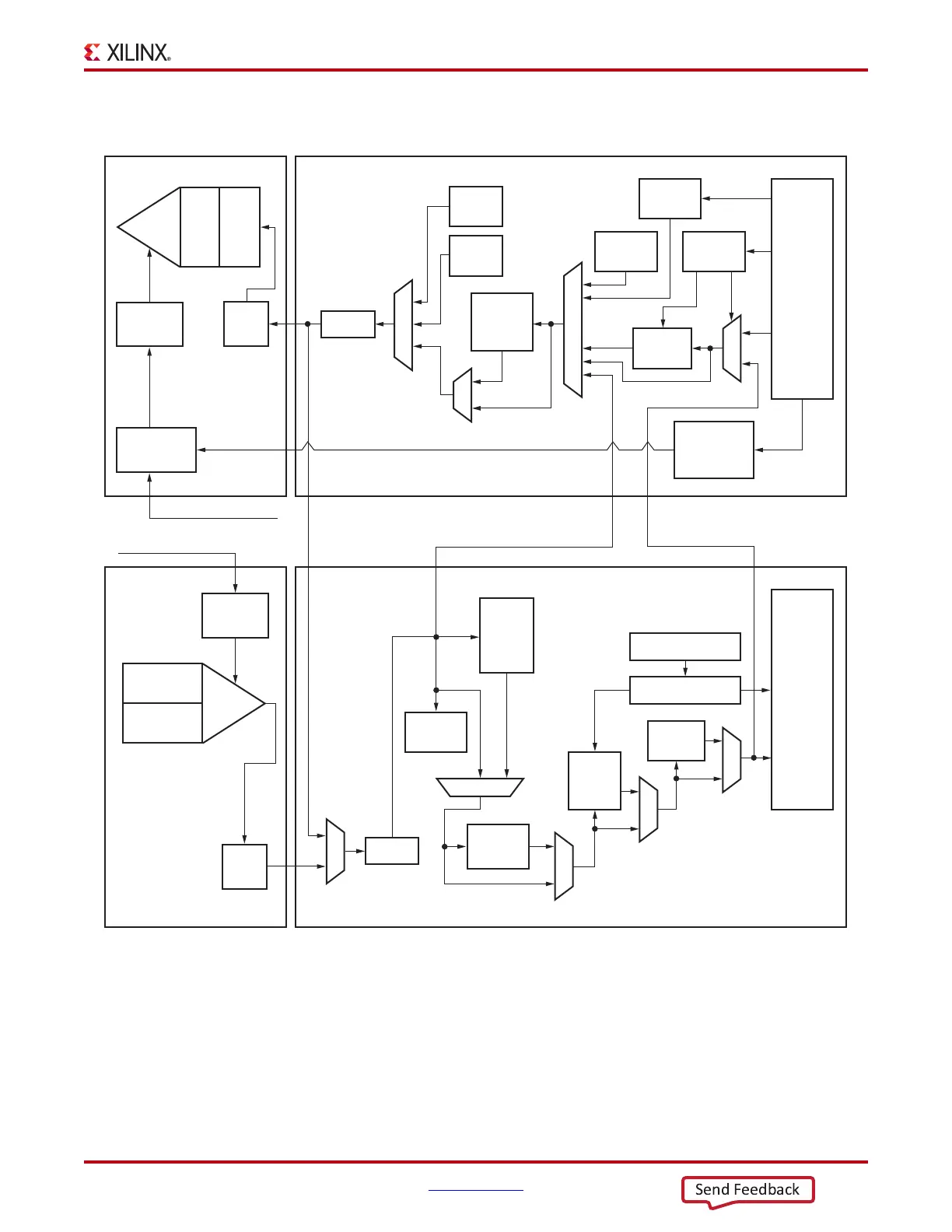
Figure 1-3 illustrates the topology of a GTPE2_CHANNEL primitive.
Refer to Figure 2-9, page 35 for the description of the channel clocking architecture, which provides
clocks to the RX and TX clock dividers.
X-Ref Target - Figure 1-3
Figure 1-3: GTPE2_CHANNEL Primitive Topology
TX-PMA TX-PCS
FPGA
TX
Interface
TX
Gearbox
UG482_c1_03_110811
TX PIPE
Control
Phase
Adjust
FIFO
PCIe
Beacon
From RX Parallel Data
(Far-End PMA Loopback)
To RX Parallel
Data (Near-End
PCS Loopback)
Clock From PLL0 or PLL1
Clock From PLL0 or PLL1
From RX Parallel Data
(Far-End PCS Loopback)
PISO
TX
Pre/
Post
Emp
TX Clock
Dividers
TX Phase
Interpolator
TX Phase
Interpolator
Controller
TX
OOB
and
PCIe
TX
Driver
Polarity
Polarity
SATA
OOB
8B/10B
Encoder
Pattern
Generator
FPGA
RX
Interface
RX PIPE Control
RX Status Control
SIPO
RX OOB
RX EQ
RX
Gearbox
RX
Elastic
Buffer
PRBS
Checker
Comma
Detect
And
Align
8B/10B
Decoder
RX Clock
Dividers