EasyManua.ls Logo

Xilinx 7 Series User Manual

Xilinx 7 Series
306 pages
To Next Page IconTo Next Page
To Previous Page IconTo Previous Page
Page #151 background imageLoading...
Page #151 background image
7 Series FPGAs GTP Transceivers User Guide www.xilinx.com 151
UG482 (v1.9) December 19, 2016
RX Margin Analysis
Eye Scan Theory
RXDATA is recovered from the equalized differential waveform by sampling after the RX
equalizer. The horizontal sampling position is determined by the CDR function and the vertical
position is differential zero. This is indicated as data sample in Figure 4-20.
To enable eye scan functionality, an additional sampler is provided with programmable (horizontal
and vertical) offsets from the data sample point. This is indicated as offset sample in Figure 4-20.
A single eye scan measurement consists of accumulating the number of data samples (sample count)
and the number of times that the offset sample disagreed with the data sample (error count). The bit
error ratio (BER) at the programmed vertical and horizontal offset is the ratio of the error count to
the sample count. The sample count can range from tens of thousands to greater than 10
14
.
Repeating such BER measurements for the full array of horizontal and vertical offsets (or a
subsampled set of offsets) produces a BER map as shown in Figure 4-20, commonly referred to as
a statistical eye, where the color map represents log
10
(BER). In this view, the eye is apparently
smaller than a traditional oscilloscope view (as in Figure 4-20) because it has been closed by very
low probability jitter and noise that does not show up in the much lower number of samples of an
oscilloscope.
Because this functionality puts no restrictions on the data patterns being received nor requires any
changes in the RX settings, it can be performed while application data is being received without
error. Furthermore, no FPGA logic is required—only the ability to read and write attributes.
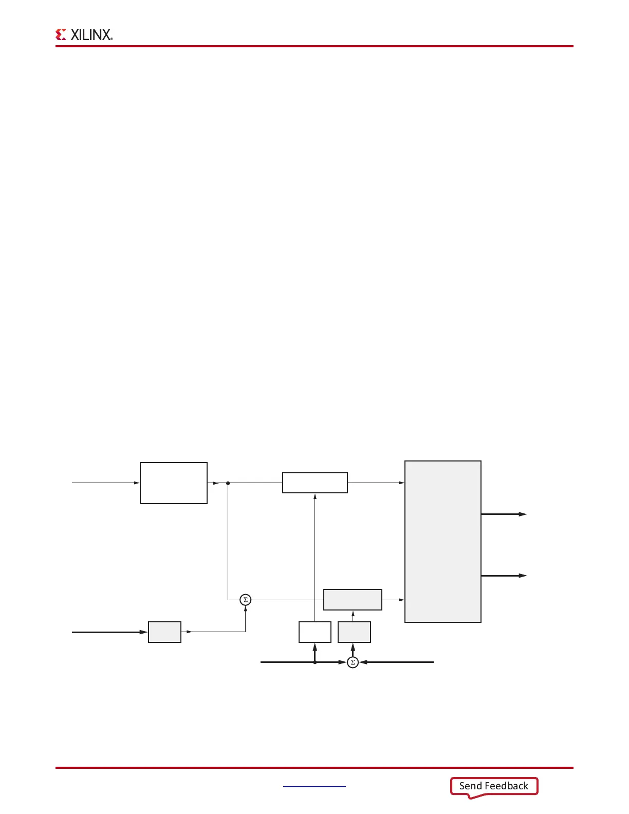
Eye Scan Architecture
The blocks with shaded gray in Figure 4-21 describe the portion of the PMA architecture that
supports eye scan. The horizontal offset (HORZ_OFFSET) advances or delays the sampling time of
the offset samples relative to the data samples. The vertical offset (VERT_OFFSET) raises or lowers
the differential voltage threshold to which the equalized waveform is compared. The data samples
are deserialized into the Rdata bus, and the offset samples are deserialized into the Sdata bus.
X-Ref Target - Figure 4-21
Figure 4-21: PMA Architecture to Support Eye Scan
UG482_c4_10_112811
Capture FF
RX Input
Equalization
Error-detection,
Screening
De-serialization
PCS
Interface
Capture FF
+
DAC PI PI
VERT_OFFSET
Rec Clock HORZ_OFFSET
Rdata
Sdata
Send Feedback

Table of Contents

Question and Answer IconNeed help?

Do you have a question about the Xilinx 7 Series and is the answer not in the manual?

Xilinx 7 Series Specifications

General IconGeneral
Process Technology28nm
TransceiversUp to 96
I/O PinsUp to 1, 200
Transceiver Data RateUp to 28.05 Gbps
Power ConsumptionVaries by device
Operating TemperatureCommercial, Industrial
Package OptionsBGA, CSP
FamilyArtix-7, Kintex-7, Virtex-7
DSP Slices16 - 3600

Summary

Chapter 1: Transceiver and Tool Overview

Overview and Features

Summary of GTP transceiver features and capabilities, including data rate and protocol support.

7 Series FPGAs Transceivers Wizard

Details on using the Wizard to generate GTP transceiver instantiation wrappers.

Simulation

Prerequisites and considerations for simulating GTP transceiver designs.

Implementation

Information on mapping GTP transceivers to device resources and creating UCF files.

Chapter 2: Shared Features

Reference Clock Input Structure

Description of the reference clock input buffer and its internal structure.

Reference Clock Selection and Distribution

Options for reference clock input, routing, and selection for GTP transceivers.

PLL

Details on the ring oscillator PLLs (PLL0 and PLL1) within the GTP Quad.

Reset and Initialization

Procedure for initializing the GTP transceiver after FPGA configuration.

Reset Modes

Explanation of sequential and single reset modes for GTP transceiver operation.

PLL Reset

Procedure for resetting the PLLs (PLL0 and PLL1) before use.

TX Initialization and Reset

Details on the TX reset state machine and its operation.

RX Initialization and Reset

Overview of RX initialization and reset processes, including sequential and single modes.

Power Down

Description of power-down modes for GTP transceiver channels and PLLs.

Loopback

Configuration and functionality of loopback modes for transceiver testing.

Dynamic Reconfiguration Port

Interface for dynamically changing parameters of GTPE2_CHANNEL and GTPE2_COMMON primitives.

Digital Monitor

Visibility into adaptation loops and convergence states for link optimization.

Chapter 3: Transmitter

TX Overview

Introduction to the GTP transceiver transmitter's functional blocks.

FPGA TX Interface

The FPGA's gateway to the TX datapath, including interface width and clocking.

TX 8B/10B Encoder

Functionality, bit/byte ordering, and K characters for 8B/10B encoding.

TX Gearbox

Support for 64B/66B and 64B/67B encoding for high-speed data protocols.

TX Buffer

Description of the TX buffer and phase alignment circuit for resolving clock domain differences.

TX Buffer Bypass

Advanced feature for adjusting phase difference and TX delay alignment.

TX Pattern Generator

Generation of PRBS and other test patterns for signal integrity testing.

TX Configurable Driver

Features of the TX driver, including voltage control, pre-emphasis, and termination.

TX Receiver Detect Support for PCI Express Designs

Feature for the transmitter to detect receiver presence on a link.

TX Out-of-Band Signaling

Support for OOB sequences in SATA/SAS and beaconing in PCI Express.

Chapter 4: Receiver

RX Overview

Introduction to the GTP transceiver receiver's functional blocks.

RX Analog Front End

Description of the RX analog front end buffer with configurable termination.

RX Out-of-Band Signaling

Support for OOB sequences in SATA/SAS and beaconing in PCI Express.

RX Equalizer

Power-efficient adaptive CTLE for compensating signal distortion.

RX CDR

Clock and data recovery circuit architecture and operation.

RX Fabric Clock Output Control

Control of serial and parallel clock dividers for the RX datapath.

RX Margin Analysis

Mechanism to measure and visualize receiver eye margin after equalization.

RX Polarity Control

Functionality to invert the polarity of incoming data.

RX Pattern Checker

Built-in PRBS checker for testing signal integrity.

RX Byte and Word Alignment

Process of aligning serial data to symbol boundaries for parallel data usage.

RX 8B/10B Decoder

Decoding of 8B/10B encoded data, including features and error handling.

RX Buffer Bypass

Advanced feature to bypass the RX elastic buffer for reduced latency.

RX Elastic Buffer

Functionality of the RX elastic buffer for resolving clock domain phase differences.

RX Clock Correction

Mechanism to bridge clock domain differences and prevent buffer overflow/underflow.

RX Channel Bonding

Feature to cancel skew between lanes by adjusting RX elastic buffer latency.

RX Gearbox

Support for 64B/66B and 64B/67B header and payload separation.

FPGA RX Interface

The FPGA's gateway to the RX datapath, including port widths and clocking.

Chapter 5: Board Design Guidelines

Overview

Introduction to implementing GTP transceiver designs on printed circuit boards.

Pin Description and Design Guidelines

Guidelines for routing GTP transceiver signals and managing SelectIO activity.

GTP Pin Descriptions

Detailed description of GTP Quad pins and their functions.

Termination Resistor Calibration Circuit

Description of the RCAL circuit for resistor calibration.

Analog Power Supply Pins

Discussion of MGTAVCC and MGTAVTT power planes and their organization.

Reference Clock

Selection criteria for reference clock sources and oscillators.

Power Supply and Filtering

Considerations for analog power supplies, regulators, and filtering.

PCB Design Checklist

A checklist for designing and reviewing GTP transceiver PCB schematics and layouts.

Appendix A: Placement Information by Package

CPG236 Package Placement Diagram

Placement diagram for the CPG236 package, showing GTP transceiver locations.

CSG325 Package Placement Diagram

Placement diagram for the CSG325 package, showing GTP transceiver locations.

CLG485 Package Placement Diagram

Placement diagram for the CLG485 package, showing GTP transceiver locations.

FGG484 Package Placement Diagram

Placement diagram for the FGG484 package, showing GTP transceiver locations.

FGG676 Package Placement Diagram

Placement diagram for the FGG676 package, showing GTP transceiver locations.

FBG484 Package Placement Diagram

Placement diagram for the FBG484 package, showing GTP transceiver locations.

SBG484 Package Placement Diagram

Placement diagram for the SBG484 package, showing GTP transceiver locations.

FFG1156 Package Placement Diagram

Placement diagram for the FFG1156 package, showing GTP transceiver locations.

Appendix B: Placement Information by Device

Appendix C: 8B/10B Valid Characters

Appendix D: DRP Address Map of the GTP Transceiver

Related product manuals