7 Series FPGAs GTP Transceivers User Guide www.xilinx.com 209
UG482 (v1.9) December 19, 2016
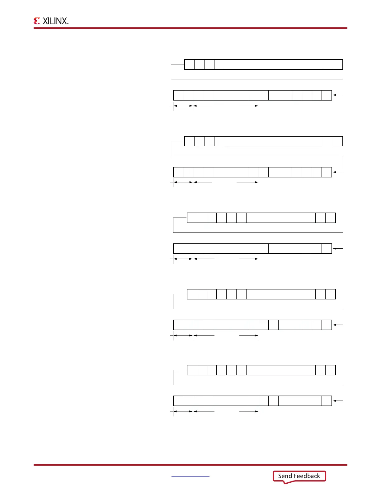
RX Gearbox
X-Ref Target - Figure 4-54
Figure 4-54: RX Gearbox Operation
D15 D14 D5 D4 D3 D2……………
D15 D14 D3 D2
………………………
D0 …………D15
D1 D0
D1 D0 D15 D14 D5 D4………………
D1 D0
D15 D14 D3 D2………………………
D0 ………
D15 D14 D5 D4 D3 D2………………
D1 D0 D5………………………
D0 …………D15
D4
D1 D0 D15 D14 D6 D5 D4………………
D3 D2 D5………………
D0 …………
D1 D0
D4D15 D14
D15
D3 D2
H1 H0
H1 H0
H1
H1 H0
D15
D14
D1 D0
H0
Input to the RXGearbox
Cycle N
Cycle N+3
RXHEADEROUTVALID = 1'b1
RXDATAOUTVALID = 1'b1
RXHEADER RXDATA
Input to the RXGearbox
Cycle N+1
RXHEADEROUTVALID = 1'b0
RXDATAOUTVALID = 1'b1
RXHEADER RXDATA
Input to the RXGearbox
Cycle N+2
RXHEADEROUTVALID = 1'b0
RXDATAOUTVALID = 1'b1
RXHEADER RXDATA
Input to the RXGearbox
RXHEADEROUTVALID = 1'b0
RXDATAOUTVALID = 1'b1
RXHEADER
RXDATA
Output of the
RXGearbox
Output of the
RXGearbox
Output of the
RXGearbox
Output of the
RXGearbox
UG482_c4_36_111011
D15 D14 D4………………
D3 D2
D1 D0 D5………………
D0 …………
D15 D14
D4
Cycle N+4
Input to the RXGearbox
RXHEADEROUTVALID = 1'b1
RXDATAOUTVALID = 1'b1
RXHEADER
RXDATA
Output of the
RXGearbox
D15 D14
 Loading...


