210 www.xilinx.com 7 Series FPGAs GTP Transceivers User Guide
UG482 (v1.9) December 19, 2016
Chapter 4: Receiver
Note relevant to Figure 4-54:
1. As per IEEE Std 802.3ae-2002 nomenclature, H1 corresponds to RxB<0>, H0 to RxB<1>, etc.
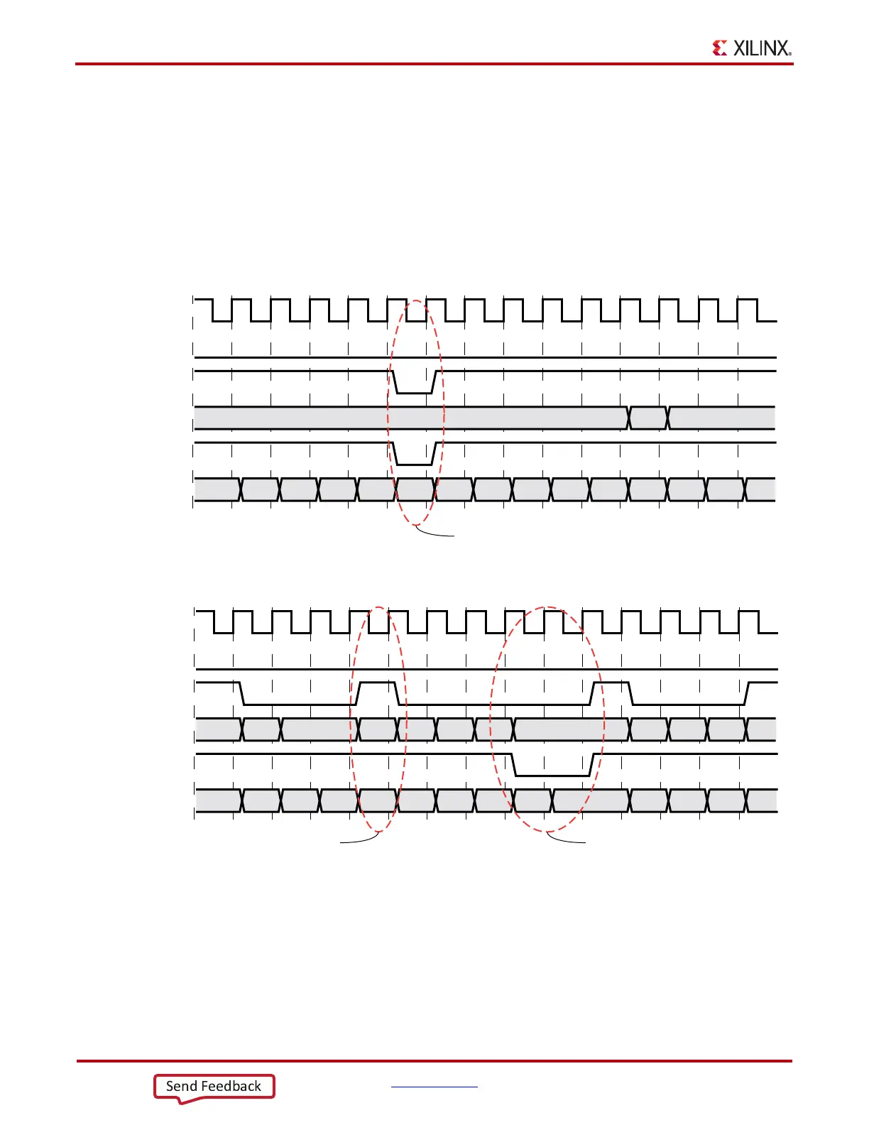
The RX gearbox internally manages all sequencing, which differs from the TX gearbox option of
either internal or external sequencing. Depending on whether a 2-byte or 4-byte interface is used,
RXDATAOUTVALID and RXHEADEROUTVALID assert and deassert for different periods of
length. The RX gearbox encounters similar data and header pauses found in the TX gearbox.
Figure 4-55 shows such a pause in addition to RXHEADERVALID and RXDATAVALID being
deasserted for one cycle. Figure 4-56 shows the operation for 64B/67B encoding when
RX_DATA_WIDTH = 16 (2-byte).
RX Gearbox Block Synchronization
The 64B/66B and 64B/67B protocols depend on block synchronization to determine their block
boundaries. Block synchronization is required because all incoming data is unaligned before block
lock is achieved. The goal is to search for the valid synchronization header by changing the data
alignment. The RXGEARBOXSLIP input port is used to change the gearbox data alignment so that
all possible alignments can be checked. The RXGEARBOXSLIP signal feeds back from the block
X-Ref Target - Figure 4-55
Figure 4-55: RX Gearbox When Using 64B/66B Encoding and RX_DATA_WIDTH = 32 (4-Byte)
UG482_c4_37_111011
1
D
a
D
b
D
c
D
d
D
e
XXX D
f
D
g
D
h
D
i
D
j
D
k
D
l
D
m
D
n
12
RXUSRCLK2
RXGEARBOXSLIP
RXHEADERVALID
RXHEADER[1:0]
RXDATAVALID
RXDATA[63:0]
Data pauses for 1 cycle.
X-Ref Target - Figure 4-56
Figure 4-56: RX Gearbox When Using 64B/67B Encoding and RX_DATA_WIDTH = 16 (2-Byte)
UG482_c4_38_111011
11 110066 62
D
a
D
b
D
c
D
d
D
e
XXXD
f
D
g
D
h
D
i
D
j
D
k
D
l
D
m
50
RXUSRCLK2
RXGEARBOXSLIP
RXHEADERVALID
RXHEADER[2:0]
RXDATAVALID
RXDATA[15:0]
Data pauses for 1 cycle. Data pauses for 2 cycles.
 Loading...


