266 www.xilinx.com 7 Series FPGAs GTP Transceivers User Guide
UG482 (v1.9) December 19, 2016
Appendix D: DRP Address Map of the GTP Transceiver
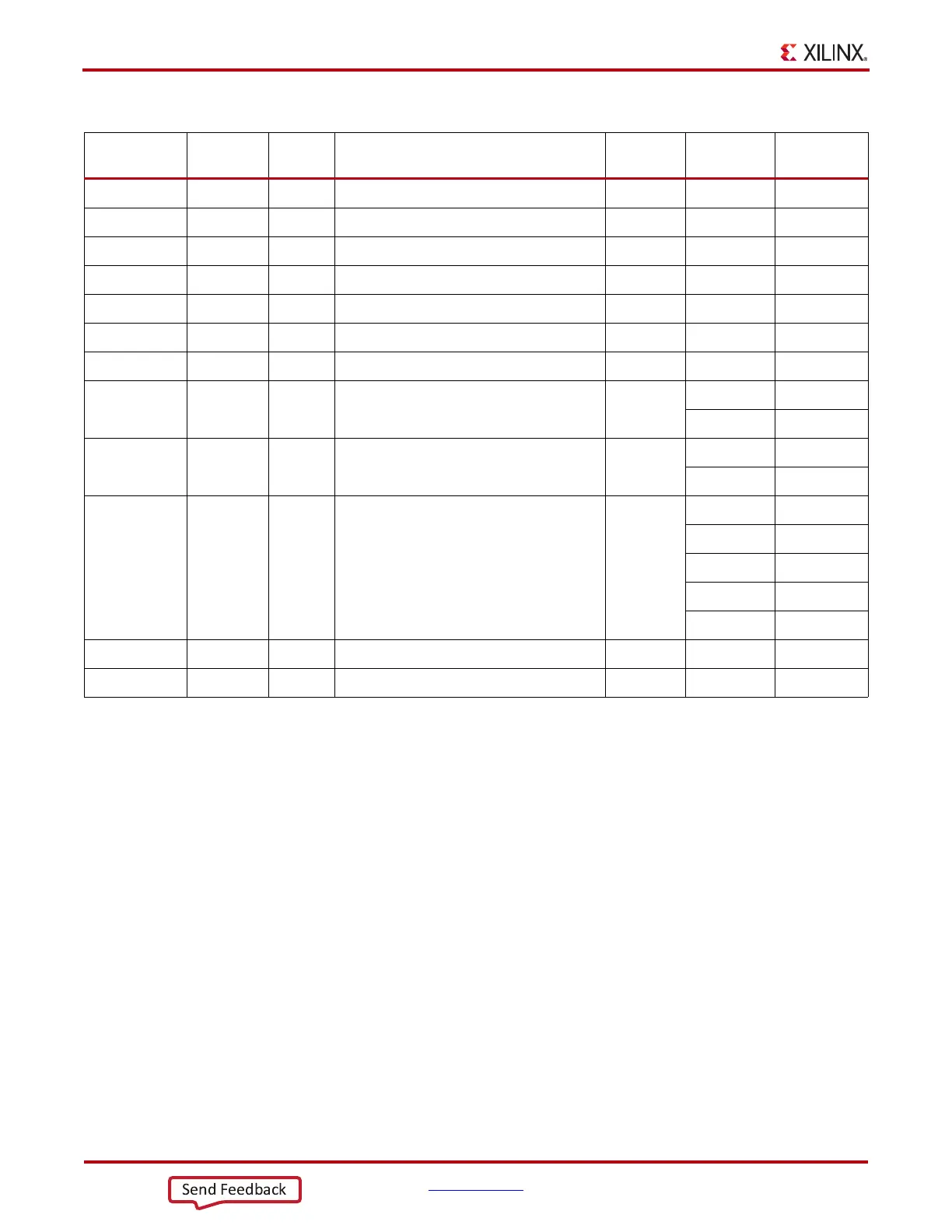
001A 15:0 R/W BIAS_CFG 31:16 0-65535 0-65535
001B 15:0 R/W BIAS_CFG 47:32 0-65535 0-65535
001C 15:0 R/W BIAS_CFG 63:48 0-65535 0-65535
0024 15:0 R/W RSVD_ATTR1 15:0 0-65535 0-65535
0028 15:0 R/W PLL1_INIT_CFG 15:0 0-65535 0-65535
0029 7:0 R/W PLL1_INIT_CFG 23:16 0-255 0-255
002A 8:0 R/W PLL1_LOCK_CFG 8:0 0-511 0-511
002B 13:9 R/W PLL1_REFCLK_DIV 4:0
116
20
002B 7 R/W PLL1_FBDIV_45 0
40
51
002B 5:0 R/W PLL1_FBDIV 5:0
116
20
31
42
53
002C 15:0 R/W PLL1_CFG 15:0 0-65535 0-65535
002D 10:0 R/W PLL1_CFG 26:16 0-2047 0-2047
Table D-1: DRP Map of GTPE2_COMMON Primitive (Cont’d)
DRP Address
(Hex)
DRP Bits R/W Attribute Name
Attribute
Bits
Attribute
Encoding
DRP Binary
Encoding