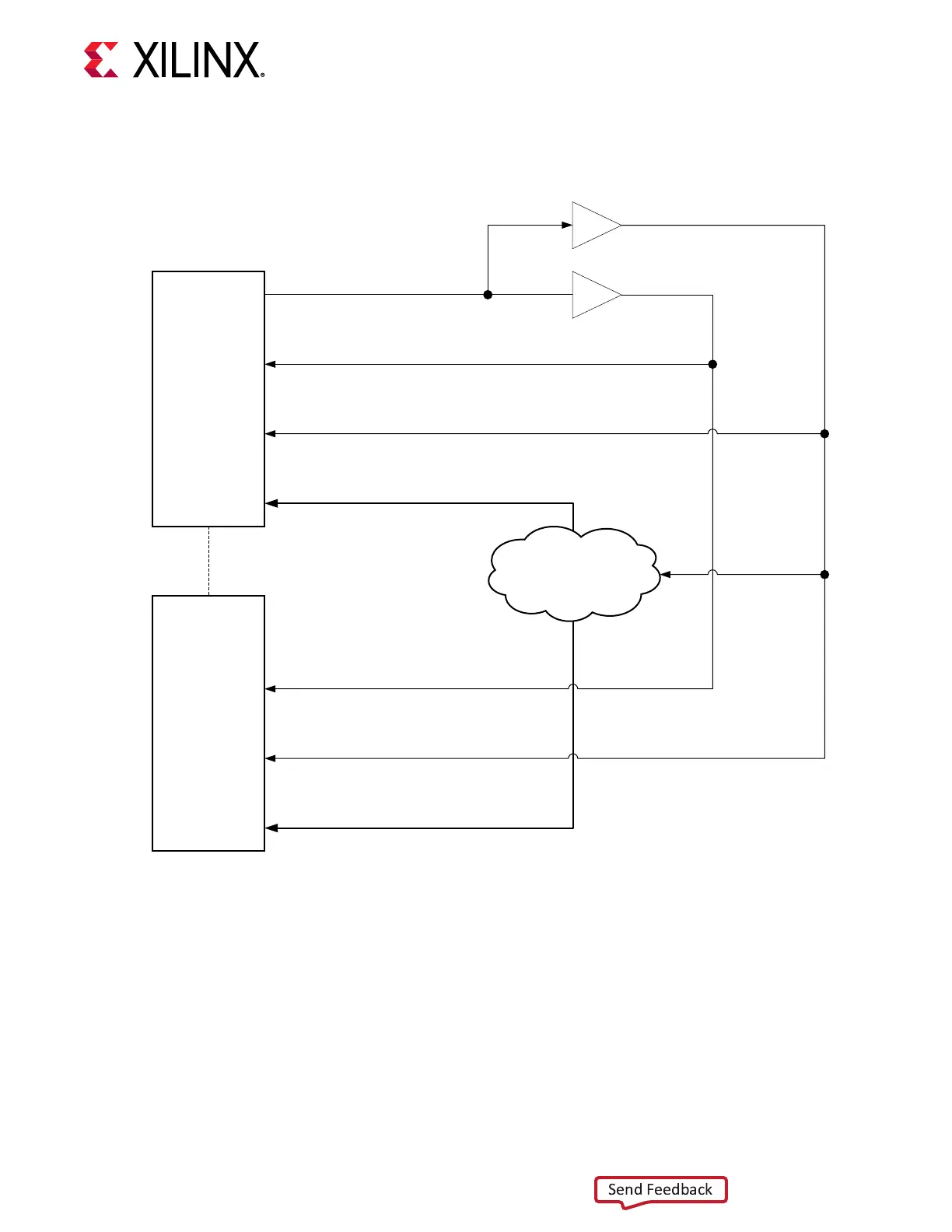
Figure 29: Multiple Lanes—TXPROGDIVCLK Drives TXUSRCLK and TXUSRCLK2 (128-Bit,
160-Bit, or 256-Bit Mode)
Design in UltraScale
Architecture
÷1
UltraScale
Devices GTM
Transceiver
TXPROGDIVCLK
BUFG_GT
1
TXUSRCLK2
2
TXUSRCLK
2
TXDATA (TX data width = 128/160/256 bits)
÷2
BUFG_GT
1
UltraScale
Devices GTM
Transceiver
TXDATA (TX data width = 128/160/256 bits)
TXUSRCLK2
2
TXUSRCLK
2
X20918-111918
Notes relevant to the gure:
1. For details about placement constraints and restricons on clocking resources (BUFG_GT,
BUFG_GT_SYNC, etc.), refer to the UltraScale Architecture Clocking Resources User Guide
(UG572).
2. F
TXUSRCLK2
= F
TXUSRCLK
/2.
Chapter 3: Transmitter
UG581 (v1.0) January 4, 2019 www.xilinx.com
Virtex UltraScale+ GTM Transceivers 62
 Loading...

